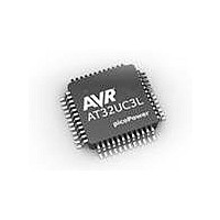
AT32UC3L032-D3UR Atmel, AT32UC3L032-D3UR Datasheet - Page 79

AT32UC3L032-D3UR
Manufacturer Part Number
AT32UC3L032-D3UR
Description
MCU AVR32 32KB FLASH 48TLLGA
Manufacturer
Atmel
Series
AVR®32 UC3r
Datasheet
1.AT32UC3L-EK.pdf
(858 pages)
Specifications of AT32UC3L032-D3UR
Core Processor
AVR
Core Size
32-Bit
Speed
50MHz
Connectivity
I²C, SPI, UART/USART
Peripherals
Brown-out Detect/Reset, DMA, PWM, WDT
Number Of I /o
36
Program Memory Size
32KB (32K x 8)
Program Memory Type
FLASH
Ram Size
16K x 8
Voltage - Supply (vcc/vdd)
1.62 V ~ 3.6 V
Data Converters
A/D 9x10b
Oscillator Type
Internal
Operating Temperature
-40°C ~ 85°C
Package / Case
48-TLLGA
Processor Series
AT32UC3x
Core
AVR32
Data Bus Width
32 bit
Data Ram Size
16 KB
Interface Type
SPI, TWI, USART
Maximum Clock Frequency
50 MHz
Number Of Programmable I/os
36
Number Of Timers
7
Maximum Operating Temperature
+ 85 C
Mounting Style
SMD/SMT
3rd Party Development Tools
EWAVR32, EWAVR32-BL
Development Tools By Supplier
AT32UC3L-EK
Minimum Operating Temperature
- 40 C
On-chip Adc
10 bit, 9 Channel
Lead Free Status / RoHS Status
Lead free / RoHS Compliant
Eeprom Size
-
Lead Free Status / Rohs Status
Details
- Current page: 79 of 858
- Download datasheet (13Mb)
32099F–11/2010
also the other word in the same 64-bit location is read. The first word is output on the bus, and
the other word is put into an internal buffer. If a read to a sequential address is to be performed
in the next cycle, the buffered word is output on the bus, while the next 64-bit location is read
from the flash memory. Thus, latency in 1 wait state mode is hidden for sequential fetches.
The programmer can select the wait states required by writing to the FWS field in the Flash Con-
trol Register (FCR). It is the responsibility of the programmer to select a number of wait states
compatible with the clock frequency and timing characteristics of the flash memory.
In 0ws mode, no wait states are encountered on any flash read operations. In 1 ws mode, one
stall cycle is encountered on the first access in a single or burst transfer. In 1 ws mode, if the first
access in a burst access is to an address that is not 64-bit aligned, an additional stall cycle is
also encountered when reading the second word in the burst. All subsequent words in the burst
are accessed without any stall cycles.
The Flash Controller provides two sets of buffers that can be enabled in order to speed up
instruction fetching. These buffers can be enabled by writing a one to the FCR.SEQBUF and
FCR.BRBUF bits. The SEQBUF bit enables buffering hardware optimizing sequential instruction
fetches. The BRBUF bit enables buffering hardware optimizing tight inner loops. These buffers
are never used when the flash is in 0 wait state mode. Usually, both these buffers should be
enabled when operating in 1 wait state mode. Some users requiring absolute cycle determinism
may want to keep the buffers disabled.
The Flash Controller address space is displayed in
address pw and the User page is reserved, and reading addresses in this space returns an
undefined result. The User page is permanently mapped to an offset of 0x00800000 from the
start address of the flash memory.
Table 8-1.
Memory type
Main array
User
User Page Addresses
Start address, byte sized
0
0x00800000
Size
pw words = 4pw bytes
64 words = 256 bytes
Figure
AT32UC3L016/32/64
8-1. The memory space between
79
Related parts for AT32UC3L032-D3UR
Image
Part Number
Description
Manufacturer
Datasheet
Request
R

Part Number:
Description:
KIT DEV/EVAL FOR AT32UC3L0
Manufacturer:
Atmel
Datasheet:

Part Number:
Description:
DEV KIT FOR AVR/AVR32
Manufacturer:
Atmel
Datasheet:

Part Number:
Description:
INTERVAL AND WIPE/WASH WIPER CONTROL IC WITH DELAY
Manufacturer:
ATMEL Corporation
Datasheet:

Part Number:
Description:
Low-Voltage Voice-Switched IC for Hands-Free Operation
Manufacturer:
ATMEL Corporation
Datasheet:

Part Number:
Description:
MONOLITHIC INTEGRATED FEATUREPHONE CIRCUIT
Manufacturer:
ATMEL Corporation
Datasheet:

Part Number:
Description:
AM-FM Receiver IC U4255BM-M
Manufacturer:
ATMEL Corporation
Datasheet:

Part Number:
Description:
Monolithic Integrated Feature Phone Circuit
Manufacturer:
ATMEL Corporation
Datasheet:

Part Number:
Description:
Multistandard Video-IF and Quasi Parallel Sound Processing
Manufacturer:
ATMEL Corporation
Datasheet:

Part Number:
Description:
High-performance EE PLD
Manufacturer:
ATMEL Corporation
Datasheet:

Part Number:
Description:
8-bit Flash Microcontroller
Manufacturer:
ATMEL Corporation
Datasheet:

Part Number:
Description:
2-Wire Serial EEPROM
Manufacturer:
ATMEL Corporation
Datasheet:


