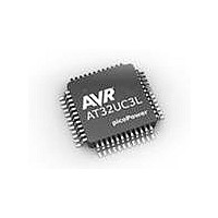
AT32UC3L032-D3UR Atmel, AT32UC3L032-D3UR Datasheet - Page 604

AT32UC3L032-D3UR
Manufacturer Part Number
AT32UC3L032-D3UR
Description
MCU AVR32 32KB FLASH 48TLLGA
Manufacturer
Atmel
Series
AVR®32 UC3r
Datasheet
1.AT32UC3L-EK.pdf
(858 pages)
Specifications of AT32UC3L032-D3UR
Core Processor
AVR
Core Size
32-Bit
Speed
50MHz
Connectivity
I²C, SPI, UART/USART
Peripherals
Brown-out Detect/Reset, DMA, PWM, WDT
Number Of I /o
36
Program Memory Size
32KB (32K x 8)
Program Memory Type
FLASH
Ram Size
16K x 8
Voltage - Supply (vcc/vdd)
1.62 V ~ 3.6 V
Data Converters
A/D 9x10b
Oscillator Type
Internal
Operating Temperature
-40°C ~ 85°C
Package / Case
48-TLLGA
Processor Series
AT32UC3x
Core
AVR32
Data Bus Width
32 bit
Data Ram Size
16 KB
Interface Type
SPI, TWI, USART
Maximum Clock Frequency
50 MHz
Number Of Programmable I/os
36
Number Of Timers
7
Maximum Operating Temperature
+ 85 C
Mounting Style
SMD/SMT
3rd Party Development Tools
EWAVR32, EWAVR32-BL
Development Tools By Supplier
AT32UC3L-EK
Minimum Operating Temperature
- 40 C
On-chip Adc
10 bit, 9 Channel
Lead Free Status / RoHS Status
Lead free / RoHS Compliant
Eeprom Size
-
Lead Free Status / Rohs Status
Details
- Current page: 604 of 858
- Download datasheet (13Mb)
26.6.6
26.6.7
26.6.8
26.6.9
32099F–11/2010
ADC Clock
ADC Sleep Mode
Startup Time
Sample and Hold Time
The Pseudorandom Noise Generator is always enabled when a conversion is in progress, but
the line can be multiplexed with other I/O Controller lines. In this case, the user must make sure
the I/O Controller is configured correctly to allow the noise signal to propagate out to the PRND
pin.
The PRND pin is updated with a new value from the Pseudorandom Noise Generator with inter-
vals given by the following equation:
T
Note that the observed period on the PRND pin will depend on the number of consecutive zeros
or ones that are made by the Pseudorandom Noise Generator.
The ADCIFB generates an internal clock named CLK_ADC that is used by the Analog-to-Digital
Converter cell to perform conversions. The CLK_ADC frequency is selected by writing to the
PRESCAL field in the ADC Configuration Register (ACR). The CLK_ADC range is between
CLK_ADCIFB/2, if PRESCAL is 0, and CLK_ADCIFB/128, if PRESCAL is 63 (0x3F).
A sensible PRESCAL value must be used in order to provide an ADC clock frequency according
to the maximum sampling rate parameter given in the Electrical Characteristics section. Failing
to do so may result in incorrect Analog-to-Digital Converter operation.
The ADC Sleep Mode maximizes power saving by automatically deactivating the Analog-to-Dig-
ital Converter cell when it is not being used for conversions. The ADC Sleep Mode is enabled by
writing a one to the SLEEP bit in the ADC Configuration Register (ACR).
When a trigger occurs while the ADC Sleep Mode is enabled, the Analog-to-Digital Converter
cell is automatically activated. As the analog cell requires a startup time, the logic waits during
this time and then starts the conversion of the enabled channels. When conversions of all
enabled channels are complete, the ADC is deactivated until the next trigger.
The Analog-to-Digital Converter cell has a minimal startup time when the cell is activated. This
startup time is given in the Electrical Characteristics chapter and must be written to the
STARTUP field in the ADC Configuration Register (ACR) to get correct conversion results.
The STARTUP field expects the startup time to be represented as the number of CLK_ADC
cycles between 8 and 1024 and in steps of 8 that is needed to cover the ADC startup time as
specified in the Electrical Characteristics chapter.
The Analog-to-Digital Converter cell is activated at the first conversion after reset and remains
active if ACR.SLEEP is zero. If ACR.SLEEP is one, the Analog-to-Digital Converter cell is auto-
matically deactivated when idle and thus each conversion sequence will have a initial startup
time delay.
A minimal Sample and Hold Time is necessary for the ADCIFB to guarantee the best converted
final value when switching between ADC channels. This time depends on the input impedance
of the analog input, but also on the output impedance of the driver providing the signal to the
analog input, as there is no input buffer amplifier.
PRND
= (PRESCAL[5:3]+1) * 2 * TCLK_ADCIFB
AT32UC3L016/32/64
604
Related parts for AT32UC3L032-D3UR
Image
Part Number
Description
Manufacturer
Datasheet
Request
R

Part Number:
Description:
KIT DEV/EVAL FOR AT32UC3L0
Manufacturer:
Atmel
Datasheet:

Part Number:
Description:
DEV KIT FOR AVR/AVR32
Manufacturer:
Atmel
Datasheet:

Part Number:
Description:
INTERVAL AND WIPE/WASH WIPER CONTROL IC WITH DELAY
Manufacturer:
ATMEL Corporation
Datasheet:

Part Number:
Description:
Low-Voltage Voice-Switched IC for Hands-Free Operation
Manufacturer:
ATMEL Corporation
Datasheet:

Part Number:
Description:
MONOLITHIC INTEGRATED FEATUREPHONE CIRCUIT
Manufacturer:
ATMEL Corporation
Datasheet:

Part Number:
Description:
AM-FM Receiver IC U4255BM-M
Manufacturer:
ATMEL Corporation
Datasheet:

Part Number:
Description:
Monolithic Integrated Feature Phone Circuit
Manufacturer:
ATMEL Corporation
Datasheet:

Part Number:
Description:
Multistandard Video-IF and Quasi Parallel Sound Processing
Manufacturer:
ATMEL Corporation
Datasheet:

Part Number:
Description:
High-performance EE PLD
Manufacturer:
ATMEL Corporation
Datasheet:

Part Number:
Description:
8-bit Flash Microcontroller
Manufacturer:
ATMEL Corporation
Datasheet:

Part Number:
Description:
2-Wire Serial EEPROM
Manufacturer:
ATMEL Corporation
Datasheet:


