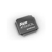
AT32UC3L032-D3UR Atmel, AT32UC3L032-D3UR Datasheet - Page 728

AT32UC3L032-D3UR
Manufacturer Part Number
AT32UC3L032-D3UR
Description
MCU AVR32 32KB FLASH 48TLLGA
Manufacturer
Atmel
Series
AVR®32 UC3r
Datasheet
1.AT32UC3L-EK.pdf
(858 pages)
Specifications of AT32UC3L032-D3UR
Core Processor
AVR
Core Size
32-Bit
Speed
50MHz
Connectivity
I²C, SPI, UART/USART
Peripherals
Brown-out Detect/Reset, DMA, PWM, WDT
Number Of I /o
36
Program Memory Size
32KB (32K x 8)
Program Memory Type
FLASH
Ram Size
16K x 8
Voltage - Supply (vcc/vdd)
1.62 V ~ 3.6 V
Data Converters
A/D 9x10b
Oscillator Type
Internal
Operating Temperature
-40°C ~ 85°C
Package / Case
48-TLLGA
Processor Series
AT32UC3x
Core
AVR32
Data Bus Width
32 bit
Data Ram Size
16 KB
Interface Type
SPI, TWI, USART
Maximum Clock Frequency
50 MHz
Number Of Programmable I/os
36
Number Of Timers
7
Maximum Operating Temperature
+ 85 C
Mounting Style
SMD/SMT
3rd Party Development Tools
EWAVR32, EWAVR32-BL
Development Tools By Supplier
AT32UC3L-EK
Minimum Operating Temperature
- 40 C
On-chip Adc
10 bit, 9 Channel
Lead Free Status / RoHS Status
Lead free / RoHS Compliant
Eeprom Size
-
Lead Free Status / Rohs Status
Details
- Current page: 728 of 858
- Download datasheet (13Mb)
31. Programming and Debugging
31.1
31.2
31.2.1
32099F–11/2010
Overview
Service Access Bus
SAB Address Map
The AT32UC3L supports programming and debugging through two interfaces, JTAG or aWire
JTAG is an industry standard interface and allows boundary scan for PCB testing, as well as
daisy-chaining of multiple devices on the PCB. aWire is an Atmel proprietary protocol which
offers higher throughput and robust communication, and does not require application pins to be
reserved. Either interface provides access to the internal Service Access Bus (SAB), which
offers a bridge to the High Speed Bus, giving access to memories and peripherals in the device.
By using this bridge to the bus system, the flash and fuses can thus be programmed by access-
ing the Flash Controller in the same manner as the CPU.
The SAB also provides access to the Nexus-compliant On-Chip Debug (OCD) system in the
device, which gives the user non-intrusive run-time control of the program execution. Addition-
ally, trace information can be output on the Auxiliary (AUX) debug port or buffered in internal
RAM for later retrieval by JTAG or aWire.
The AVR32 architecture offers a common interface for access to On-Chip Debug, programming,
and test functions. These are mapped on a common bus called the Service Access Bus (SAB),
which is linked to the JTAG and aWire port through a bus master module, which also handles
synchronization between the debugger and SAB clocks.
When accessing the SAB through the debugger there are no limitations on debugger frequency
compared to chip frequency, although there must be an active system clock in order for the SAB
accesses to complete. If the system clock is switched off in sleep mode, activity on the debugger
will restart the system clock automatically, without waking the device from sleep. Debuggers
may optimize the transfer rate by adjusting the frequency in relation to the system clock. This
ratio can be measured with debug protocol specific instructions.
The Service Access Bus uses 36 address bits to address memory or registers in any of the
slaves on the bus. The bus supports sized accesses of bytes (8 bits), halfwords (16 bits), or
words (32 bits). All accesses must be aligned to the size of the access, i.e. halfword accesses
must have the lowest address bit cleared, and word accesses must have the two lowest address
bits cleared.
The Service Access Bus (SAB) gives the user access to the internal address space and other
features through a 36 bits address space. The 4 MSBs identify the slave number, while the 32
LSBs are decoded within the slave’s address space. The SAB slaves are shown in
Table 31-1.
Unallocated
Slave
OCD
HSB
SAB Slaves, Addresses and Descriptions
Address [35:32]
0x0
0x1
0x4
Description
Intentionally unallocated
OCD registers
HSB memory space, as seen by the CPU
AT32UC3L016/32/64
Table
31-1.
728
™
.
Related parts for AT32UC3L032-D3UR
Image
Part Number
Description
Manufacturer
Datasheet
Request
R

Part Number:
Description:
KIT DEV/EVAL FOR AT32UC3L0
Manufacturer:
Atmel
Datasheet:

Part Number:
Description:
DEV KIT FOR AVR/AVR32
Manufacturer:
Atmel
Datasheet:

Part Number:
Description:
INTERVAL AND WIPE/WASH WIPER CONTROL IC WITH DELAY
Manufacturer:
ATMEL Corporation
Datasheet:

Part Number:
Description:
Low-Voltage Voice-Switched IC for Hands-Free Operation
Manufacturer:
ATMEL Corporation
Datasheet:

Part Number:
Description:
MONOLITHIC INTEGRATED FEATUREPHONE CIRCUIT
Manufacturer:
ATMEL Corporation
Datasheet:

Part Number:
Description:
AM-FM Receiver IC U4255BM-M
Manufacturer:
ATMEL Corporation
Datasheet:

Part Number:
Description:
Monolithic Integrated Feature Phone Circuit
Manufacturer:
ATMEL Corporation
Datasheet:

Part Number:
Description:
Multistandard Video-IF and Quasi Parallel Sound Processing
Manufacturer:
ATMEL Corporation
Datasheet:

Part Number:
Description:
High-performance EE PLD
Manufacturer:
ATMEL Corporation
Datasheet:

Part Number:
Description:
8-bit Flash Microcontroller
Manufacturer:
ATMEL Corporation
Datasheet:

Part Number:
Description:
2-Wire Serial EEPROM
Manufacturer:
ATMEL Corporation
Datasheet:


