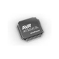
AT32UC3L032-D3UR Atmel, AT32UC3L032-D3UR Datasheet - Page 45

AT32UC3L032-D3UR
Manufacturer Part Number
AT32UC3L032-D3UR
Description
MCU AVR32 32KB FLASH 48TLLGA
Manufacturer
Atmel
Series
AVR®32 UC3r
Datasheet
1.AT32UC3L-EK.pdf
(858 pages)
Specifications of AT32UC3L032-D3UR
Core Processor
AVR
Core Size
32-Bit
Speed
50MHz
Connectivity
I²C, SPI, UART/USART
Peripherals
Brown-out Detect/Reset, DMA, PWM, WDT
Number Of I /o
36
Program Memory Size
32KB (32K x 8)
Program Memory Type
FLASH
Ram Size
16K x 8
Voltage - Supply (vcc/vdd)
1.62 V ~ 3.6 V
Data Converters
A/D 9x10b
Oscillator Type
Internal
Operating Temperature
-40°C ~ 85°C
Package / Case
48-TLLGA
Processor Series
AT32UC3x
Core
AVR32
Data Bus Width
32 bit
Data Ram Size
16 KB
Interface Type
SPI, TWI, USART
Maximum Clock Frequency
50 MHz
Number Of Programmable I/os
36
Number Of Timers
7
Maximum Operating Temperature
+ 85 C
Mounting Style
SMD/SMT
3rd Party Development Tools
EWAVR32, EWAVR32-BL
Development Tools By Supplier
AT32UC3L-EK
Minimum Operating Temperature
- 40 C
On-chip Adc
10 bit, 9 Channel
Lead Free Status / RoHS Status
Lead free / RoHS Compliant
Eeprom Size
-
Lead Free Status / Rohs Status
Details
- Current page: 45 of 858
- Download datasheet (13Mb)
7.5.10
7.5.11
7.5.12
7.6
7.6.1
32099F–11/2010
Performance Monitors
Priority
Error Handling
Peripheral Event Trigger
Measuring mechanisms
If more than one PDCA channel is requesting transfer at a given time, the PDCA channels are
prioritized by their channel number. Channels with lower numbers have priority over channels
with higher numbers, giving channel zero the highest priority.
If the Memory Address Register (MAR) is set to point to an invalid location in memory, an error
will occur when the PDCA tries to perform a transfer. When an error occurs, the Transfer Error
bit in the Interrupt Status Register (ISR.TERR) will be set and the DMA channel that caused the
error will be stopped. In order to restart the channel, the user must program the Memory
Address Register to a valid address and then write a one to the Error Clear bit in the Control
Register (CR.ECLR). If the Transfer Error interrupt is enabled, an interrupt request will be gener-
ated when an transfer error occurs.
Peripheral events can be used to trigger PDCA channel transfers. Peripheral Event synchroniza-
tions are enabled by writing a one to the Event Trigger bit in the Mode Register (MR.ETRIG).
When set, all DMA requests will be blocked until an peripheral event is received. For each
peripheral event received, only one data item is transferred. If no DMA requests are pending
when a peripheral event is received, the PDCA will start a transfer as soon as a peripheral event
is detected. If multiple events arrive while the PDCA channel is busy transferring data, an over-
flow condition will be signaled in the Peripheral Event System. Refer to the Peripheral Event
System chapter for more information.
Up tp two performance monitors allow the user to measure the activity and stall cycles for PDCA
transfers. To monitor a PDCA channel, the corresponding channel number must be written to
one of the MONnCH fields in the Performance Control Register (PCONTROL) and a one must
be written to the corresponding CHnEN bit in the same register.
Due to performance monitor hardware resource sharing, the two monitor channels should NOT
be programmed to monitor the same PDCA channel. This may result in UNDEFINED perfor-
mance monitor behavior.
Three different parameters can be measured by each channel:
These measurements can be extracted by software and used to generate indicators for bus
latency, bus load, and maximum bus latency.
Each of the counters has a fixed width, and may therefore overflow. When an overflow is
encountered in either the Performance Channel Data Read/Write Cycle registers (PRDATAn
and PWDATAn) or the Performance Channel Read/Write Stall Cycles registers (PRSTALLn and
PWSTALLn) of a channel, all registers in the channel are reset. This behavior is altered if the
Channel Overflow Freeze bit is one in the Performance Control register (PCONTROL.CHnOVF).
If this bit is one, the channel registers are frozen when either DATA or STALL reaches its maxi-
mum value. This simplifies one-shot readout of the counter values.
• The number of data transfer cycles since last channel reset, both for read and write
• The number of stall cycles since last channel reset, both for read and write
• The maximum latency since last channel reset, both for read and write
AT32UC3L016/32/64
45
Related parts for AT32UC3L032-D3UR
Image
Part Number
Description
Manufacturer
Datasheet
Request
R

Part Number:
Description:
KIT DEV/EVAL FOR AT32UC3L0
Manufacturer:
Atmel
Datasheet:

Part Number:
Description:
DEV KIT FOR AVR/AVR32
Manufacturer:
Atmel
Datasheet:

Part Number:
Description:
INTERVAL AND WIPE/WASH WIPER CONTROL IC WITH DELAY
Manufacturer:
ATMEL Corporation
Datasheet:

Part Number:
Description:
Low-Voltage Voice-Switched IC for Hands-Free Operation
Manufacturer:
ATMEL Corporation
Datasheet:

Part Number:
Description:
MONOLITHIC INTEGRATED FEATUREPHONE CIRCUIT
Manufacturer:
ATMEL Corporation
Datasheet:

Part Number:
Description:
AM-FM Receiver IC U4255BM-M
Manufacturer:
ATMEL Corporation
Datasheet:

Part Number:
Description:
Monolithic Integrated Feature Phone Circuit
Manufacturer:
ATMEL Corporation
Datasheet:

Part Number:
Description:
Multistandard Video-IF and Quasi Parallel Sound Processing
Manufacturer:
ATMEL Corporation
Datasheet:

Part Number:
Description:
High-performance EE PLD
Manufacturer:
ATMEL Corporation
Datasheet:

Part Number:
Description:
8-bit Flash Microcontroller
Manufacturer:
ATMEL Corporation
Datasheet:

Part Number:
Description:
2-Wire Serial EEPROM
Manufacturer:
ATMEL Corporation
Datasheet:


