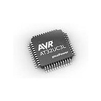
AT32UC3L032-D3UR Atmel, AT32UC3L032-D3UR Datasheet - Page 82

AT32UC3L032-D3UR
Manufacturer Part Number
AT32UC3L032-D3UR
Description
MCU AVR32 32KB FLASH 48TLLGA
Manufacturer
Atmel
Series
AVR®32 UC3r
Datasheet
1.AT32UC3L-EK.pdf
(858 pages)
Specifications of AT32UC3L032-D3UR
Core Processor
AVR
Core Size
32-Bit
Speed
50MHz
Connectivity
I²C, SPI, UART/USART
Peripherals
Brown-out Detect/Reset, DMA, PWM, WDT
Number Of I /o
36
Program Memory Size
32KB (32K x 8)
Program Memory Type
FLASH
Ram Size
16K x 8
Voltage - Supply (vcc/vdd)
1.62 V ~ 3.6 V
Data Converters
A/D 9x10b
Oscillator Type
Internal
Operating Temperature
-40°C ~ 85°C
Package / Case
48-TLLGA
Processor Series
AT32UC3x
Core
AVR32
Data Bus Width
32 bit
Data Ram Size
16 KB
Interface Type
SPI, TWI, USART
Maximum Clock Frequency
50 MHz
Number Of Programmable I/os
36
Number Of Timers
7
Maximum Operating Temperature
+ 85 C
Mounting Style
SMD/SMT
3rd Party Development Tools
EWAVR32, EWAVR32-BL
Development Tools By Supplier
AT32UC3L-EK
Minimum Operating Temperature
- 40 C
On-chip Adc
10 bit, 9 Channel
Lead Free Status / RoHS Status
Lead free / RoHS Compliant
Eeprom Size
-
Lead Free Status / Rohs Status
Details
- Current page: 82 of 858
- Download datasheet (13Mb)
32099F–11/2010
Figure 8-3.
Internally, the flash memory stores data in 64-bit doublewords. Therefore, the native data size of
the Page Buffer is also a 64-bit doubleword. All locations shown in
bleword locations. Since the HSB bus only has a 32-bit data width, two 32-bit HSB transfers
must be performed to write a 64-bit doubleword into the Page Buffer. The FLASHCDW has logic
to combine two 32-bit HSB transfers into a 64-bit data before writing this 64-bit data into the
Page Buffer. This logic requires the word with the low address to be written to the HSB bus
before the word with the high address. To exemplify, to write a 64-bit value to doubleword X0
residing in page X, first write a 32-bit word to the byte address pointing to address X0, thereafter
write a word to the byte address pointing to address (X0+4).
The page buffer is word-addressable and should only be written with aligned word transfers,
never with byte or halfword transfers. The page buffer can not be read.
The page buffer is also used for writes to the User page.
Page buffer write operations are performed with 4 wait states. Any accesses attempted to the
FLASHCDW on the HSB bus during these cycles will be automatically stalled.
Writing to the page buffer can only change page buffer bits from one to zero, i.e. writing
0xAAAAAAAA to a page buffer location that has the value 0x00000000 will not change the page
buffer value. The only way to change a bit from zero to one is to erase the entire page buffer with
the Clear Page Buffer command.
All locations are doubleword locations
31
27
23
19
15
11
7
3
Page Buffer
30
26
22
18
14
10
Mapping from Page Buffer to Flash
64-bit data
6
2
29
25
21
17
13
9
5
1
28
24
20
16
12
8
4
0
Y31
Y27
Y23
Y19
Y15
Y11
X31
X27
X23
X19
X15
X11
Z31
Z27
Z23
Z19
Z15
Z11
Y7
Y3
X7
X3
Z7
Z3
AT32UC3L016/32/64
Z30
Z26
Z22
Z18
Z14
Z10
Y30
Y26
Y22
Y18
Y14
Y10
X30
X26
X22
X18
X14
X10
Y6
Y2
X6
X2
Z6
Z2
Page Y
Page X
Page Z
Flash
Figure 8-3
Z29
Z25
Z21
Z17
Z13
Y29
Y25
Y21
Y17
Y13
X29
X25
X21
X17
X13
Y9
Y5
Y1
X9
X5
X1
Z9
Z5
Z1
are therefore dou-
Z28
Z24
Z20
Z16
Z12
Y28
Y24
Y20
Y16
Y12
X28
X24
X20
X16
X12
Z8
Z4
Z0
Y8
Y4
Y0
X8
X4
X0
82
Related parts for AT32UC3L032-D3UR
Image
Part Number
Description
Manufacturer
Datasheet
Request
R

Part Number:
Description:
KIT DEV/EVAL FOR AT32UC3L0
Manufacturer:
Atmel
Datasheet:

Part Number:
Description:
DEV KIT FOR AVR/AVR32
Manufacturer:
Atmel
Datasheet:

Part Number:
Description:
INTERVAL AND WIPE/WASH WIPER CONTROL IC WITH DELAY
Manufacturer:
ATMEL Corporation
Datasheet:

Part Number:
Description:
Low-Voltage Voice-Switched IC for Hands-Free Operation
Manufacturer:
ATMEL Corporation
Datasheet:

Part Number:
Description:
MONOLITHIC INTEGRATED FEATUREPHONE CIRCUIT
Manufacturer:
ATMEL Corporation
Datasheet:

Part Number:
Description:
AM-FM Receiver IC U4255BM-M
Manufacturer:
ATMEL Corporation
Datasheet:

Part Number:
Description:
Monolithic Integrated Feature Phone Circuit
Manufacturer:
ATMEL Corporation
Datasheet:

Part Number:
Description:
Multistandard Video-IF and Quasi Parallel Sound Processing
Manufacturer:
ATMEL Corporation
Datasheet:

Part Number:
Description:
High-performance EE PLD
Manufacturer:
ATMEL Corporation
Datasheet:

Part Number:
Description:
8-bit Flash Microcontroller
Manufacturer:
ATMEL Corporation
Datasheet:

Part Number:
Description:
2-Wire Serial EEPROM
Manufacturer:
ATMEL Corporation
Datasheet:


