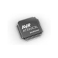
AT32UC3L032-D3UR Atmel, AT32UC3L032-D3UR Datasheet - Page 44

AT32UC3L032-D3UR
Manufacturer Part Number
AT32UC3L032-D3UR
Description
MCU AVR32 32KB FLASH 48TLLGA
Manufacturer
Atmel
Series
AVR®32 UC3r
Datasheet
1.AT32UC3L-EK.pdf
(858 pages)
Specifications of AT32UC3L032-D3UR
Core Processor
AVR
Core Size
32-Bit
Speed
50MHz
Connectivity
I²C, SPI, UART/USART
Peripherals
Brown-out Detect/Reset, DMA, PWM, WDT
Number Of I /o
36
Program Memory Size
32KB (32K x 8)
Program Memory Type
FLASH
Ram Size
16K x 8
Voltage - Supply (vcc/vdd)
1.62 V ~ 3.6 V
Data Converters
A/D 9x10b
Oscillator Type
Internal
Operating Temperature
-40°C ~ 85°C
Package / Case
48-TLLGA
Processor Series
AT32UC3x
Core
AVR32
Data Bus Width
32 bit
Data Ram Size
16 KB
Interface Type
SPI, TWI, USART
Maximum Clock Frequency
50 MHz
Number Of Programmable I/os
36
Number Of Timers
7
Maximum Operating Temperature
+ 85 C
Mounting Style
SMD/SMT
3rd Party Development Tools
EWAVR32, EWAVR32-BL
Development Tools By Supplier
AT32UC3L-EK
Minimum Operating Temperature
- 40 C
On-chip Adc
10 bit, 9 Channel
Lead Free Status / RoHS Status
Lead free / RoHS Compliant
Eeprom Size
-
Lead Free Status / Rohs Status
Details
- Current page: 44 of 858
- Download datasheet (13Mb)
7.5.5
7.5.6
7.5.7
7.5.8
7.5.9
32099F–11/2010
Ring Buffer
Peripheral Selection
Transfer Size
Enabling and Disabling
Interrupts
If TCR is zero when writing to TCRR, the TCR and MAR are automatically updated with the
value written in TCRR and MARR.
When Ring Buffer mode is enabled the TCRR and MARR registers will not be cleared when
TCR and MAR registers reload. This allows the PDCA to read or write to the same memory
region over and over again until the transfer is actively stopped by the user. Ring Buffer mode is
enabled by writing a one to the Ring Buffer bit in the Mode Register (MR.RING).
The Peripheral Select Register (PSR) decides which peripheral should be connected to the
PDCA channel. A peripheral is selected by writing the corresponding Peripheral Identity (PID) to
the PID field in the PSR register. Writing the PID will both select the direction of the transfer
(memory to peripheral or peripheral to memory), which handshake interface to use, and the
address of the peripheral holding register. Refer to the Peripheral Identity (PID) table in the Mod-
ule Configuration section for the peripheral PID values.
The transfer size can be set individually for each channel to be either byte, halfword or word (8-
bit, 16-bit or 32-bit respectively). Transfer size is set by writing the desired value to the Transfer
Size field in the Mode Register (MR.SIZE).
When the PDCA moves data between peripherals and memory, data is automatically sized and
aligned. When memory is accessed, the size specified in MR.SIZE and system alignment is
used. When a peripheral register is accessed the data to be transferred is converted to a word
where bit n in the data corresponds to bit n in the peripheral register. If the transfer size is byte or
halfword, bits greater than 8 and16 respectively are set to zero.
Refer to the Module Configuration section for information regarding what peripheral registers are
used for the different peripherals and then to the peripheral specific chapter for information
about the size option available for the different registers.
Each DMA channel is enabled by writing a one to the Transfer Enable bit in the Control Register
(CR.TEN) and disabled by writing a one to the Transfer Disable bit (CR.TDIS). The current sta-
tus can be read from the Status Register (SR).
While the PDCA channel is enabled all DMA request will be handled as long the TCR and TCRR
is not zero.
Interrupts can be enabled by writing a one to the corresponding bit in the Interrupt Enable Regis-
ter (IER) and disabled by writing a one to the corresponding bit in the Interrupt Disable Register
(IDR). The Interrupt Mask Register (IMR) can be read to see whether an interrupt is enabled or
not. The current status of an interrupt source can be read through the Interrupt Status Register
(ISR).
The PDCA has three interrupt sources:
• Reload Counter Zero - The TCRR register is zero.
• Transfer Finished - Both the TCR and TCRR registers are zero.
• Transfer Error - An error has occurred in accessing memory.
AT32UC3L016/32/64
44
Related parts for AT32UC3L032-D3UR
Image
Part Number
Description
Manufacturer
Datasheet
Request
R

Part Number:
Description:
KIT DEV/EVAL FOR AT32UC3L0
Manufacturer:
Atmel
Datasheet:

Part Number:
Description:
DEV KIT FOR AVR/AVR32
Manufacturer:
Atmel
Datasheet:

Part Number:
Description:
INTERVAL AND WIPE/WASH WIPER CONTROL IC WITH DELAY
Manufacturer:
ATMEL Corporation
Datasheet:

Part Number:
Description:
Low-Voltage Voice-Switched IC for Hands-Free Operation
Manufacturer:
ATMEL Corporation
Datasheet:

Part Number:
Description:
MONOLITHIC INTEGRATED FEATUREPHONE CIRCUIT
Manufacturer:
ATMEL Corporation
Datasheet:

Part Number:
Description:
AM-FM Receiver IC U4255BM-M
Manufacturer:
ATMEL Corporation
Datasheet:

Part Number:
Description:
Monolithic Integrated Feature Phone Circuit
Manufacturer:
ATMEL Corporation
Datasheet:

Part Number:
Description:
Multistandard Video-IF and Quasi Parallel Sound Processing
Manufacturer:
ATMEL Corporation
Datasheet:

Part Number:
Description:
High-performance EE PLD
Manufacturer:
ATMEL Corporation
Datasheet:

Part Number:
Description:
8-bit Flash Microcontroller
Manufacturer:
ATMEL Corporation
Datasheet:

Part Number:
Description:
2-Wire Serial EEPROM
Manufacturer:
ATMEL Corporation
Datasheet:


