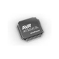
AT32UC3L032-D3UR Atmel, AT32UC3L032-D3UR Datasheet - Page 746

AT32UC3L032-D3UR
Manufacturer Part Number
AT32UC3L032-D3UR
Description
MCU AVR32 32KB FLASH 48TLLGA
Manufacturer
Atmel
Series
AVR®32 UC3r
Datasheet
1.AT32UC3L-EK.pdf
(858 pages)
Specifications of AT32UC3L032-D3UR
Core Processor
AVR
Core Size
32-Bit
Speed
50MHz
Connectivity
I²C, SPI, UART/USART
Peripherals
Brown-out Detect/Reset, DMA, PWM, WDT
Number Of I /o
36
Program Memory Size
32KB (32K x 8)
Program Memory Type
FLASH
Ram Size
16K x 8
Voltage - Supply (vcc/vdd)
1.62 V ~ 3.6 V
Data Converters
A/D 9x10b
Oscillator Type
Internal
Operating Temperature
-40°C ~ 85°C
Package / Case
48-TLLGA
Processor Series
AT32UC3x
Core
AVR32
Data Bus Width
32 bit
Data Ram Size
16 KB
Interface Type
SPI, TWI, USART
Maximum Clock Frequency
50 MHz
Number Of Programmable I/os
36
Number Of Timers
7
Maximum Operating Temperature
+ 85 C
Mounting Style
SMD/SMT
3rd Party Development Tools
EWAVR32, EWAVR32-BL
Development Tools By Supplier
AT32UC3L-EK
Minimum Operating Temperature
- 40 C
On-chip Adc
10 bit, 9 Channel
Lead Free Status / RoHS Status
Lead free / RoHS Compliant
Eeprom Size
-
Lead Free Status / Rohs Status
Details
- Current page: 746 of 858
- Download datasheet (13Mb)
31.4.11.1
31.4.11.2
31.4.11.3
31.4.11.4
32099F–11/2010
SAB Address Mode
Block Transfer
Canceling a SAB Access
Busy Reporting
which is linked to the JTAG through a bus master module, which also handles synchronization
between the TCK and SAB clocks.
For more information about the SAB and a list of SAB slaves see the Service Access Bus
chapter.
The MEMORY_SIZED_ACCESS instruction allows a sized read or write to any 36-bit address
on the bus. MEMORY_WORD_ACCESS is a shorthand instruction for 32-bit accesses to any
36-bit address, while the NEXUS_ACCESS instruction is a Nexus-compliant shorthand instruc-
tion for accessing the 32-bit OCD registers in the 7-bit address space reserved for these. These
instructions require two passes through the Shift-DR TAP state: one for the address and control
information, and one for data.
To increase the transfer rate, consecutive memory accesses can be accomplished by the
MEMORY_BLOCK_ACCESS instruction, which only requires a single pass through Shift-DR for
data transfer only. The address is automatically incremented according to the size of the last
SAB transfer.
It is possible to abort an ongoing SAB access by the CANCEL_ACCESS instruction, to avoid
hanging the bus due to an extremely slow slave.
As the time taken to perform an access may vary depending on system activity and current chip
frequency, all the SAB access JTAG instructions can return a busy indicator. This indicates
whether a delay needs to be inserted, or an operation needs to be repeated in order to be suc-
cessful. If a new access is requested while the SAB is busy, the request is ignored.
The SAB becomes busy when:
The SAB becomes ready again when:
What to do if the busy bit is set:
• Entering Update-DR in the address phase of any read operation, e.g., after scanning in a
• Entering Update-DR in the data phase of any write operation, e.g., after scanning in data for
• Entering Update-DR during a MEMORY_BLOCK_ACCESS.
• Entering Update-DR after scanning in a counter value for SYNC.
• Entering Update-IR after scanning in a MEMORY_BLOCK_ACCESS if the previous access
• A read or write operation completes.
• A SYNC countdown completed.
• A operation is cancelled by the CANCEL_ACCESS instruction.
• During Shift-IR: The new instruction is selected, but the previous operation has not yet
NEXUS_ACCESS address with the read bit set.
a NEXUS_ACCESS write.
was a read and data was scanned after scanning the address.
completed and will continue (unless the new instruction is CANCEL_ACCESS). You may
AT32UC3L016/32/64
746
Related parts for AT32UC3L032-D3UR
Image
Part Number
Description
Manufacturer
Datasheet
Request
R

Part Number:
Description:
KIT DEV/EVAL FOR AT32UC3L0
Manufacturer:
Atmel
Datasheet:

Part Number:
Description:
DEV KIT FOR AVR/AVR32
Manufacturer:
Atmel
Datasheet:

Part Number:
Description:
INTERVAL AND WIPE/WASH WIPER CONTROL IC WITH DELAY
Manufacturer:
ATMEL Corporation
Datasheet:

Part Number:
Description:
Low-Voltage Voice-Switched IC for Hands-Free Operation
Manufacturer:
ATMEL Corporation
Datasheet:

Part Number:
Description:
MONOLITHIC INTEGRATED FEATUREPHONE CIRCUIT
Manufacturer:
ATMEL Corporation
Datasheet:

Part Number:
Description:
AM-FM Receiver IC U4255BM-M
Manufacturer:
ATMEL Corporation
Datasheet:

Part Number:
Description:
Monolithic Integrated Feature Phone Circuit
Manufacturer:
ATMEL Corporation
Datasheet:

Part Number:
Description:
Multistandard Video-IF and Quasi Parallel Sound Processing
Manufacturer:
ATMEL Corporation
Datasheet:

Part Number:
Description:
High-performance EE PLD
Manufacturer:
ATMEL Corporation
Datasheet:

Part Number:
Description:
8-bit Flash Microcontroller
Manufacturer:
ATMEL Corporation
Datasheet:

Part Number:
Description:
2-Wire Serial EEPROM
Manufacturer:
ATMEL Corporation
Datasheet:


