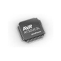
AT32UC3L032-D3UR Atmel, AT32UC3L032-D3UR Datasheet - Page 515

AT32UC3L032-D3UR
Manufacturer Part Number
AT32UC3L032-D3UR
Description
MCU AVR32 32KB FLASH 48TLLGA
Manufacturer
Atmel
Series
AVR®32 UC3r
Datasheet
1.AT32UC3L-EK.pdf
(858 pages)
Specifications of AT32UC3L032-D3UR
Core Processor
AVR
Core Size
32-Bit
Speed
50MHz
Connectivity
I²C, SPI, UART/USART
Peripherals
Brown-out Detect/Reset, DMA, PWM, WDT
Number Of I /o
36
Program Memory Size
32KB (32K x 8)
Program Memory Type
FLASH
Ram Size
16K x 8
Voltage - Supply (vcc/vdd)
1.62 V ~ 3.6 V
Data Converters
A/D 9x10b
Oscillator Type
Internal
Operating Temperature
-40°C ~ 85°C
Package / Case
48-TLLGA
Processor Series
AT32UC3x
Core
AVR32
Data Bus Width
32 bit
Data Ram Size
16 KB
Interface Type
SPI, TWI, USART
Maximum Clock Frequency
50 MHz
Number Of Programmable I/os
36
Number Of Timers
7
Maximum Operating Temperature
+ 85 C
Mounting Style
SMD/SMT
3rd Party Development Tools
EWAVR32, EWAVR32-BL
Development Tools By Supplier
AT32UC3L-EK
Minimum Operating Temperature
- 40 C
On-chip Adc
10 bit, 9 Channel
Lead Free Status / RoHS Status
Lead free / RoHS Compliant
Eeprom Size
-
Lead Free Status / Rohs Status
Details
- Current page: 515 of 858
- Download datasheet (13Mb)
22.9.1
Name:
Access Type:
Offset:
Reset Value:
• TENBIT: Ten Bit Address Match
• ADR: Slave Address
• SOAM: Stretch Clock on Address Match
• CUP: NBYTES Count Up
• ACK: Slave Receiver Data Phase ACK Value
• PECEN: Packet Error Checking Enable
• SMHH: SMBus Host Header
• SMDA: SMBus Default Address
• SMBALERT: SMBus Alert
32099F–11/2010
SWRST
31
23
15
7
-
Write this bit to zero to disable Ten Bit Address Match.
Write this bit to one to enable Ten Bit Address Match.
Slave address used in slave address match. Bits 9:0 are used if in 10-bit mode, bits 6:0 otherwise.
Writing this bit to zero will not strech bus clock after address match.
Writing this bit to one will strech bus clock after address match.
Writing this bit to zero causes NBYTES to count down (decrement) per byte transferred.
Writing this bit to one causes NBYTES to count up (increment) per byte transferred.
Writing this bit to zero causes a low value to be returned in the ACK cycle of the data phase in slave receiver mode.
Writing this bit to one causes a high value to be returned in the ACK cycle of the data phase in slave receiver mode.
Writing this bit to zero disables SMBus PEC (CRC) generation and check.
Writing this bit to one enables SMBus PEC (CRC) generation and check.
Writing this bit to zero causes TWIS not to acknowledge the SMBus Host Header.
Writing this bit to one causes TWIS to acknowledge the SMBus Host Header.
Writing this bit to zero causes TWIS not to acknowledge the SMBus Default Address.
Writing this bit to one causes TWIS to acknowledge the SMBus Default Address.
Writing this bit to zero causes TWIS to release the SMBALERT line and not to acknowledge the SMBus Alert Response
Address (ARA).
Writing this bit to one causes TWIS to pull down the SMBALERT line and to acknowledge the SMBus Alert Response Address
(ARA).
Control Register
SOAM
30
22
14
6
-
-
CR
Read/Write
0x00
0x00000000
CUP
29
21
13
5
-
-
STREN
ACK
28
20
12
4
-
ADR[7:0]
GCMATCH
PECEN
27
19
11
3
-
SMATCH
TENBIT
SMHH
26
18
10
2
AT32UC3L016/32/64
SMEN
SMDA
25
17
9
1
ADR[9:8]
SMBALERT
SEN
24
16
8
0
515
Related parts for AT32UC3L032-D3UR
Image
Part Number
Description
Manufacturer
Datasheet
Request
R

Part Number:
Description:
KIT DEV/EVAL FOR AT32UC3L0
Manufacturer:
Atmel
Datasheet:

Part Number:
Description:
DEV KIT FOR AVR/AVR32
Manufacturer:
Atmel
Datasheet:

Part Number:
Description:
INTERVAL AND WIPE/WASH WIPER CONTROL IC WITH DELAY
Manufacturer:
ATMEL Corporation
Datasheet:

Part Number:
Description:
Low-Voltage Voice-Switched IC for Hands-Free Operation
Manufacturer:
ATMEL Corporation
Datasheet:

Part Number:
Description:
MONOLITHIC INTEGRATED FEATUREPHONE CIRCUIT
Manufacturer:
ATMEL Corporation
Datasheet:

Part Number:
Description:
AM-FM Receiver IC U4255BM-M
Manufacturer:
ATMEL Corporation
Datasheet:

Part Number:
Description:
Monolithic Integrated Feature Phone Circuit
Manufacturer:
ATMEL Corporation
Datasheet:

Part Number:
Description:
Multistandard Video-IF and Quasi Parallel Sound Processing
Manufacturer:
ATMEL Corporation
Datasheet:

Part Number:
Description:
High-performance EE PLD
Manufacturer:
ATMEL Corporation
Datasheet:

Part Number:
Description:
8-bit Flash Microcontroller
Manufacturer:
ATMEL Corporation
Datasheet:

Part Number:
Description:
2-Wire Serial EEPROM
Manufacturer:
ATMEL Corporation
Datasheet:


