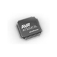
AT32UC3L032-D3UR Atmel, AT32UC3L032-D3UR Datasheet - Page 809

AT32UC3L032-D3UR
Manufacturer Part Number
AT32UC3L032-D3UR
Description
MCU AVR32 32KB FLASH 48TLLGA
Manufacturer
Atmel
Series
AVR®32 UC3r
Datasheet
1.AT32UC3L-EK.pdf
(858 pages)
Specifications of AT32UC3L032-D3UR
Core Processor
AVR
Core Size
32-Bit
Speed
50MHz
Connectivity
I²C, SPI, UART/USART
Peripherals
Brown-out Detect/Reset, DMA, PWM, WDT
Number Of I /o
36
Program Memory Size
32KB (32K x 8)
Program Memory Type
FLASH
Ram Size
16K x 8
Voltage - Supply (vcc/vdd)
1.62 V ~ 3.6 V
Data Converters
A/D 9x10b
Oscillator Type
Internal
Operating Temperature
-40°C ~ 85°C
Package / Case
48-TLLGA
Processor Series
AT32UC3x
Core
AVR32
Data Bus Width
32 bit
Data Ram Size
16 KB
Interface Type
SPI, TWI, USART
Maximum Clock Frequency
50 MHz
Number Of Programmable I/os
36
Number Of Timers
7
Maximum Operating Temperature
+ 85 C
Mounting Style
SMD/SMT
3rd Party Development Tools
EWAVR32, EWAVR32-BL
Development Tools By Supplier
AT32UC3L-EK
Minimum Operating Temperature
- 40 C
On-chip Adc
10 bit, 9 Channel
Lead Free Status / RoHS Status
Lead free / RoHS Compliant
Eeprom Size
-
Lead Free Status / Rohs Status
Details
- Current page: 809 of 858
- Download datasheet (13Mb)
Table 32-40. SPI Timing, Master Mode
Note:
32.10.4.2
32099F–11/2010
Symbol
SPI0
SPI1
SPI2
SPI3
SPI4
SPI5
1. These values are based on simulation and characterization of other AVR microcontrollers manufactured in the same pro-
cess technology. These values are not covered by test limits in production.
Slave mode
Parameter
MISO setup time before SPCK rises
MISO hold time after SPCK rises
SPCK rising to MOSI delay
MISO setup time before SPCK falls
MISO hold time after SPCK falls
SPCK falling to MOSI delay
Maximum SPI Frequency, Master Output
The maximum SPI master output frequency is given by the following formula:
Where
maximum frequency of the SPI pins. Please refer to the I/O Pin Characteristics section for the
maximum frequency of the pins.
Maximum SPI Frequency, Master Input
The maximum SPI master input frequency is given by the following formula:
Where
CPOL and NCPHA.
datasheet for
Figure 32-15. SPI Slave Mode With (CPOL= 0 and NCPHA= 1) or (CPOL= 1 and NCPHA= 0)
SPCK
MISO
MOSI
SPIn
SPIn
(1)
is the MOSI delay, SPI2 or SPI5 depending on CPOL and NCPHA.
is the MISO setup and hold time, SPI0 + SPI1 or SPI3 + SPI4 depending on
t
SPI6
VALID
.
SPI7
t
VALID
is the SPI slave response time. Please refer to the SPI slave
f
SPI8
SPCKMAX
f
SPCKMAX
3.0V to 3.6V,
Conditions
V
capacitor =
maximum
VDDIO
external
40pF
=
from
MIN f
=
----------------------------------- -
SPIn
(
PINMAX
28.4 + (t
22.8 + (t
+
1
t
VALID
AT32UC3L016/32/64
,
Min
----------- -
SPIn
0
0
CLK_SPI
CLK_SPI
1
)
)/2
)/2
Max
11.0
7.1
f
PINMAX
Units
ns
is the
809
Related parts for AT32UC3L032-D3UR
Image
Part Number
Description
Manufacturer
Datasheet
Request
R

Part Number:
Description:
KIT DEV/EVAL FOR AT32UC3L0
Manufacturer:
Atmel
Datasheet:

Part Number:
Description:
DEV KIT FOR AVR/AVR32
Manufacturer:
Atmel
Datasheet:

Part Number:
Description:
INTERVAL AND WIPE/WASH WIPER CONTROL IC WITH DELAY
Manufacturer:
ATMEL Corporation
Datasheet:

Part Number:
Description:
Low-Voltage Voice-Switched IC for Hands-Free Operation
Manufacturer:
ATMEL Corporation
Datasheet:

Part Number:
Description:
MONOLITHIC INTEGRATED FEATUREPHONE CIRCUIT
Manufacturer:
ATMEL Corporation
Datasheet:

Part Number:
Description:
AM-FM Receiver IC U4255BM-M
Manufacturer:
ATMEL Corporation
Datasheet:

Part Number:
Description:
Monolithic Integrated Feature Phone Circuit
Manufacturer:
ATMEL Corporation
Datasheet:

Part Number:
Description:
Multistandard Video-IF and Quasi Parallel Sound Processing
Manufacturer:
ATMEL Corporation
Datasheet:

Part Number:
Description:
High-performance EE PLD
Manufacturer:
ATMEL Corporation
Datasheet:

Part Number:
Description:
8-bit Flash Microcontroller
Manufacturer:
ATMEL Corporation
Datasheet:

Part Number:
Description:
2-Wire Serial EEPROM
Manufacturer:
ATMEL Corporation
Datasheet:


