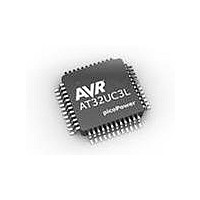
AT32UC3L032-D3UR Atmel, AT32UC3L032-D3UR Datasheet - Page 40

AT32UC3L032-D3UR
Manufacturer Part Number
AT32UC3L032-D3UR
Description
MCU AVR32 32KB FLASH 48TLLGA
Manufacturer
Atmel
Series
AVR®32 UC3r
Datasheet
1.AT32UC3L-EK.pdf
(858 pages)
Specifications of AT32UC3L032-D3UR
Core Processor
AVR
Core Size
32-Bit
Speed
50MHz
Connectivity
I²C, SPI, UART/USART
Peripherals
Brown-out Detect/Reset, DMA, PWM, WDT
Number Of I /o
36
Program Memory Size
32KB (32K x 8)
Program Memory Type
FLASH
Ram Size
16K x 8
Voltage - Supply (vcc/vdd)
1.62 V ~ 3.6 V
Data Converters
A/D 9x10b
Oscillator Type
Internal
Operating Temperature
-40°C ~ 85°C
Package / Case
48-TLLGA
Processor Series
AT32UC3x
Core
AVR32
Data Bus Width
32 bit
Data Ram Size
16 KB
Interface Type
SPI, TWI, USART
Maximum Clock Frequency
50 MHz
Number Of Programmable I/os
36
Number Of Timers
7
Maximum Operating Temperature
+ 85 C
Mounting Style
SMD/SMT
3rd Party Development Tools
EWAVR32, EWAVR32-BL
Development Tools By Supplier
AT32UC3L-EK
Minimum Operating Temperature
- 40 C
On-chip Adc
10 bit, 9 Channel
Lead Free Status / RoHS Status
Lead free / RoHS Compliant
Eeprom Size
-
Lead Free Status / Rohs Status
Details
- Current page: 40 of 858
- Download datasheet (13Mb)
6.1.4
6.1.4.1
6.1.4.2
6.2
6.2.1
6.2.2
32099F–11/2010
Startup Considerations
Power-up Sequence
Starting of Clocks
Fetching of Initial Instructions
Maximum Rise Rate
Minimum Rise Rate
To avoid risk of latch-up, the rise rate of the power supplies must not exceed the values
described in
Recommended order for power supplies is also described in this chapter.
The integrated Power-on Reset (POR33) circuitry monitoring the VDDIN powering supply
requires a minimum rise rate for the VDDIN power supply.
See
If the application can not ensure that the minimum rise rate condition for the VDDIN power sup-
ply is met, one of the following configurations can be used:
This chapter summarizes the boot sequence of the AT32UC3L. The behavior after power-up is
controlled by the Power Manager. For specific details, refer to the Power Manager chapter.
After power-up, the device will be held in a reset state by the Power-on Reset (POR18 and
POR33) circuitry for a short time to allow the power to stabilize throughout the device. After
reset, the device will use the System RC Oscillator (RCSYS) as clock source. Please refer to
Table 32-17 on page 795
On system start-up, the DFLL is disabled. All clocks to all modules are running. No clocks have
a divided frequency; all parts of the system receive a clock with the same frequency as the Sys-
tem RC Oscillator.
When powering up the device, there may be a delay before the voltage has stabilized, depend-
ing on the rise time of the supply used. The CPU can start executing code as soon as the supply
is above the POR18 and POR33 thresholds, and before the supply is stable. Before switching to
a high-speed clock source, the user should use the BOD to make sure the VDDCORE is above
the minimum level (1.62V).
After reset has been released, the AVR32 UC CPU starts fetching instructions from the reset
address, which is 0x80000000. This address points to the first address in the internal Flash.
The code read from the internal Flash is free to configure the system to use, for example, the
DFLL, to divide the frequency of the clock routed to some of the peripherals, and to gate the
clocks to unused peripherals.
• A logic “0” value is applied during power-up on pin PA11 until VDDIN rises above 1.2V.
• A logic “0” value is applied during power-up on pin RESET_N until VDDIN rises above 1.2V.
Table 32-3 on page 783
Table 32-3 on page
for the frequency for this oscillator.
for the minimum rise rate value.
783.
AT32UC3L016/32/64
40
Related parts for AT32UC3L032-D3UR
Image
Part Number
Description
Manufacturer
Datasheet
Request
R

Part Number:
Description:
KIT DEV/EVAL FOR AT32UC3L0
Manufacturer:
Atmel
Datasheet:

Part Number:
Description:
DEV KIT FOR AVR/AVR32
Manufacturer:
Atmel
Datasheet:

Part Number:
Description:
INTERVAL AND WIPE/WASH WIPER CONTROL IC WITH DELAY
Manufacturer:
ATMEL Corporation
Datasheet:

Part Number:
Description:
Low-Voltage Voice-Switched IC for Hands-Free Operation
Manufacturer:
ATMEL Corporation
Datasheet:

Part Number:
Description:
MONOLITHIC INTEGRATED FEATUREPHONE CIRCUIT
Manufacturer:
ATMEL Corporation
Datasheet:

Part Number:
Description:
AM-FM Receiver IC U4255BM-M
Manufacturer:
ATMEL Corporation
Datasheet:

Part Number:
Description:
Monolithic Integrated Feature Phone Circuit
Manufacturer:
ATMEL Corporation
Datasheet:

Part Number:
Description:
Multistandard Video-IF and Quasi Parallel Sound Processing
Manufacturer:
ATMEL Corporation
Datasheet:

Part Number:
Description:
High-performance EE PLD
Manufacturer:
ATMEL Corporation
Datasheet:

Part Number:
Description:
8-bit Flash Microcontroller
Manufacturer:
ATMEL Corporation
Datasheet:

Part Number:
Description:
2-Wire Serial EEPROM
Manufacturer:
ATMEL Corporation
Datasheet:


