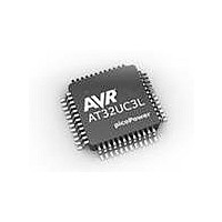
AT32UC3L032-D3UR Atmel, AT32UC3L032-D3UR Datasheet - Page 601

AT32UC3L032-D3UR
Manufacturer Part Number
AT32UC3L032-D3UR
Description
MCU AVR32 32KB FLASH 48TLLGA
Manufacturer
Atmel
Series
AVR®32 UC3r
Datasheet
1.AT32UC3L-EK.pdf
(858 pages)
Specifications of AT32UC3L032-D3UR
Core Processor
AVR
Core Size
32-Bit
Speed
50MHz
Connectivity
I²C, SPI, UART/USART
Peripherals
Brown-out Detect/Reset, DMA, PWM, WDT
Number Of I /o
36
Program Memory Size
32KB (32K x 8)
Program Memory Type
FLASH
Ram Size
16K x 8
Voltage - Supply (vcc/vdd)
1.62 V ~ 3.6 V
Data Converters
A/D 9x10b
Oscillator Type
Internal
Operating Temperature
-40°C ~ 85°C
Package / Case
48-TLLGA
Processor Series
AT32UC3x
Core
AVR32
Data Bus Width
32 bit
Data Ram Size
16 KB
Interface Type
SPI, TWI, USART
Maximum Clock Frequency
50 MHz
Number Of Programmable I/os
36
Number Of Timers
7
Maximum Operating Temperature
+ 85 C
Mounting Style
SMD/SMT
3rd Party Development Tools
EWAVR32, EWAVR32-BL
Development Tools By Supplier
AT32UC3L-EK
Minimum Operating Temperature
- 40 C
On-chip Adc
10 bit, 9 Channel
Lead Free Status / RoHS Status
Lead free / RoHS Compliant
Eeprom Size
-
Lead Free Status / Rohs Status
Details
- Current page: 601 of 858
- Download datasheet (13Mb)
26.4
Table 26-1.
26.5
26.5.1
26.5.2
26.5.3
32099F–11/2010
Pin Name
ADVREFP
TRIGGER
PRND
ADP0
ADP1
AD0-ADn
I/O Lines Description
Product Dependencies
I/O Lines
Power Management
Clocks
I/O Lines Description
In order to use this module, other parts of the system must be configured correctly, as described
below.
The analog input pins can be multiplexed with I/O Controller lines. The user must make sure the
I/O Controller is configured correctly to allow the ADCIFB access to the AD pins before the
ADCIFB is instructed to start converting data. If the user fails to do this the converted data may
be wrong.
The number of analog inputs is device dependent, please refer to the ADCIFB Module Configu-
ration chapter for the number of available AD inputs on the current device.
The ADVREFP pin must be connected correctly prior to using the ADCIFB. Failing to do so will
result in invalid ADC operation. See the Electrical Characteristics chapter for details.
If the TRIGGER, PRND, ADP0, and ADP1 pins are to be used in the application, the user must
configure the I/O Controller to assign the needed pins to the ADCIFB function.
If the CPU enters a sleep mode that disables clocks used by the ADCIFB, the ADCIFB will stop
functioning and resume operation after the system wakes up from sleep mode.
If the Peripheral Event System is configured to send asynchronous peripheral events to the
ADCIFB and the clock used by the ADCIFB is stopped, a local and temporary clock will automat-
ically be requested so the event can be processed. Refer to
and the Peripheral Event System chapter for details.
Before entering a sleep mode where the clock to the ADCIFB is stopped, make sure the Analog-
to-Digital Converter cell is put in an inactive state. Refer to
The clock for the ADCIFB bus interface (CLK_ADCIFB) is generated by the Power Manager.
This clock is enabled at reset, and can be disabled in the Power Manager. It is recommended to
disable the ADCIFB before disabling the clock, to avoid freezing the ADCIFB in an undefined
state.
Description
Reference voltage
External trigger
Pseudorandom output signal
Drive Pin 0 for Resistive Touch Screen top channel (Xp)
Drive Pin 1 for Resistive Touch Screen right channel (Yp)
Analog input channels 0 to n
AT32UC3L016/32/64
Section 26.6.14
Section
26.6.14,
Type
Analog
Digital
Digital
Digital
Digital
Analog
for more information.
Section
26.6.13,
601
Related parts for AT32UC3L032-D3UR
Image
Part Number
Description
Manufacturer
Datasheet
Request
R

Part Number:
Description:
KIT DEV/EVAL FOR AT32UC3L0
Manufacturer:
Atmel
Datasheet:

Part Number:
Description:
DEV KIT FOR AVR/AVR32
Manufacturer:
Atmel
Datasheet:

Part Number:
Description:
INTERVAL AND WIPE/WASH WIPER CONTROL IC WITH DELAY
Manufacturer:
ATMEL Corporation
Datasheet:

Part Number:
Description:
Low-Voltage Voice-Switched IC for Hands-Free Operation
Manufacturer:
ATMEL Corporation
Datasheet:

Part Number:
Description:
MONOLITHIC INTEGRATED FEATUREPHONE CIRCUIT
Manufacturer:
ATMEL Corporation
Datasheet:

Part Number:
Description:
AM-FM Receiver IC U4255BM-M
Manufacturer:
ATMEL Corporation
Datasheet:

Part Number:
Description:
Monolithic Integrated Feature Phone Circuit
Manufacturer:
ATMEL Corporation
Datasheet:

Part Number:
Description:
Multistandard Video-IF and Quasi Parallel Sound Processing
Manufacturer:
ATMEL Corporation
Datasheet:

Part Number:
Description:
High-performance EE PLD
Manufacturer:
ATMEL Corporation
Datasheet:

Part Number:
Description:
8-bit Flash Microcontroller
Manufacturer:
ATMEL Corporation
Datasheet:

Part Number:
Description:
2-Wire Serial EEPROM
Manufacturer:
ATMEL Corporation
Datasheet:


