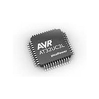
AT32UC3L032-D3UR Atmel, AT32UC3L032-D3UR Datasheet - Page 508

AT32UC3L032-D3UR
Manufacturer Part Number
AT32UC3L032-D3UR
Description
MCU AVR32 32KB FLASH 48TLLGA
Manufacturer
Atmel
Series
AVR®32 UC3r
Datasheet
1.AT32UC3L-EK.pdf
(858 pages)
Specifications of AT32UC3L032-D3UR
Core Processor
AVR
Core Size
32-Bit
Speed
50MHz
Connectivity
I²C, SPI, UART/USART
Peripherals
Brown-out Detect/Reset, DMA, PWM, WDT
Number Of I /o
36
Program Memory Size
32KB (32K x 8)
Program Memory Type
FLASH
Ram Size
16K x 8
Voltage - Supply (vcc/vdd)
1.62 V ~ 3.6 V
Data Converters
A/D 9x10b
Oscillator Type
Internal
Operating Temperature
-40°C ~ 85°C
Package / Case
48-TLLGA
Processor Series
AT32UC3x
Core
AVR32
Data Bus Width
32 bit
Data Ram Size
16 KB
Interface Type
SPI, TWI, USART
Maximum Clock Frequency
50 MHz
Number Of Programmable I/os
36
Number Of Timers
7
Maximum Operating Temperature
+ 85 C
Mounting Style
SMD/SMT
3rd Party Development Tools
EWAVR32, EWAVR32-BL
Development Tools By Supplier
AT32UC3L-EK
Minimum Operating Temperature
- 40 C
On-chip Adc
10 bit, 9 Channel
Lead Free Status / RoHS Status
Lead free / RoHS Compliant
Eeprom Size
-
Lead Free Status / Rohs Status
Details
- Current page: 508 of 858
- Download datasheet (13Mb)
Figure 22-8. Slave Transmitter with Multiple Data Bytes
22.8.4
32099F–11/2010
TCOMP
TXRDY
TWD
Slave Receiver Mode
Write THR (Data n)
NBYTES set to m
S
DADR
The TWI transfers require the receiver to acknowledge each received data byte. During the
acknowledge clock pulse (9th pulse), the slave releases the data line (HIGH), enabling the
master to pull it down in order to generate the acknowledge. The slave polls the data line dur-
ing this clock pulse and sets the NAK bit in the Status Register if the master does not
acknowledge the data byte. A NAK means that the master does not wish to receive additional
data bytes. As with the other status bits, an interrupt can be generated if enabled in the Inter-
rupt Enable Register (IER).
TXRDY is used as Transmit Ready for the Peripheral DMA Controller transmit channel.
The end of the complete transfer is marked by the SR.TCOMP bit set to one. See
on page 508
Figure 22-7. Slave Transmitter with One Data Byte
If TWIS matches an address in which the R/W bit in the TWI address phase transfer is
cleared, it will enter slave receiver mode and clear SR.TRA.
After the address phase, the following is repeated:
6. If STOP is received, SR.TCOMP and SR.STO will be set.
7. If REPEATED START is received, SR.REP will be set.
zero, and the SR.BTF bit is changed to one. The ACK indicates that more data should
be transmitted, so jump to step 2.
R
TCOMP
TXRDY
TWD
A
and
Write THR (DATA)
NBYTES set to 1
Write THR (Data n+1)
Figure 22-8 on page
S
DATA n
DADR
A
R
508.
Write THR (Data n+m)
A
DATA n+5
Last data sent
DATA
AT32UC3L016/32/64
A
DATA n+m
N
STOP sent by master
P
STOP sent by master
N
P
Figure 22-7
508
Related parts for AT32UC3L032-D3UR
Image
Part Number
Description
Manufacturer
Datasheet
Request
R

Part Number:
Description:
KIT DEV/EVAL FOR AT32UC3L0
Manufacturer:
Atmel
Datasheet:

Part Number:
Description:
DEV KIT FOR AVR/AVR32
Manufacturer:
Atmel
Datasheet:

Part Number:
Description:
INTERVAL AND WIPE/WASH WIPER CONTROL IC WITH DELAY
Manufacturer:
ATMEL Corporation
Datasheet:

Part Number:
Description:
Low-Voltage Voice-Switched IC for Hands-Free Operation
Manufacturer:
ATMEL Corporation
Datasheet:

Part Number:
Description:
MONOLITHIC INTEGRATED FEATUREPHONE CIRCUIT
Manufacturer:
ATMEL Corporation
Datasheet:

Part Number:
Description:
AM-FM Receiver IC U4255BM-M
Manufacturer:
ATMEL Corporation
Datasheet:

Part Number:
Description:
Monolithic Integrated Feature Phone Circuit
Manufacturer:
ATMEL Corporation
Datasheet:

Part Number:
Description:
Multistandard Video-IF and Quasi Parallel Sound Processing
Manufacturer:
ATMEL Corporation
Datasheet:

Part Number:
Description:
High-performance EE PLD
Manufacturer:
ATMEL Corporation
Datasheet:

Part Number:
Description:
8-bit Flash Microcontroller
Manufacturer:
ATMEL Corporation
Datasheet:

Part Number:
Description:
2-Wire Serial EEPROM
Manufacturer:
ATMEL Corporation
Datasheet:


