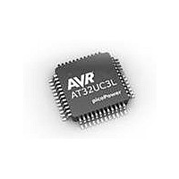
AT32UC3L032-D3UR Atmel, AT32UC3L032-D3UR Datasheet - Page 774

AT32UC3L032-D3UR
Manufacturer Part Number
AT32UC3L032-D3UR
Description
MCU AVR32 32KB FLASH 48TLLGA
Manufacturer
Atmel
Series
AVR®32 UC3r
Datasheet
1.AT32UC3L-EK.pdf
(858 pages)
Specifications of AT32UC3L032-D3UR
Core Processor
AVR
Core Size
32-Bit
Speed
50MHz
Connectivity
I²C, SPI, UART/USART
Peripherals
Brown-out Detect/Reset, DMA, PWM, WDT
Number Of I /o
36
Program Memory Size
32KB (32K x 8)
Program Memory Type
FLASH
Ram Size
16K x 8
Voltage - Supply (vcc/vdd)
1.62 V ~ 3.6 V
Data Converters
A/D 9x10b
Oscillator Type
Internal
Operating Temperature
-40°C ~ 85°C
Package / Case
48-TLLGA
Processor Series
AT32UC3x
Core
AVR32
Data Bus Width
32 bit
Data Ram Size
16 KB
Interface Type
SPI, TWI, USART
Maximum Clock Frequency
50 MHz
Number Of Programmable I/os
36
Number Of Timers
7
Maximum Operating Temperature
+ 85 C
Mounting Style
SMD/SMT
3rd Party Development Tools
EWAVR32, EWAVR32-BL
Development Tools By Supplier
AT32UC3L-EK
Minimum Operating Temperature
- 40 C
On-chip Adc
10 bit, 9 Channel
Lead Free Status / RoHS Status
Lead free / RoHS Compliant
Eeprom Size
-
Lead Free Status / Rohs Status
Details
- Current page: 774 of 858
- Download datasheet (13Mb)
31.6.7.7
31.6.7.8
31.6.7.9
32099F–11/2010
DISABLE
MEMORY_WRITE
2_PIN_MODE
the Chip Erase ongoing bit in the status bytes received after the STATUS_REQUEST
command.
Table 31-39. CHIP_ERASE Details
Disables the AW. The AW will respond with an ACK response and then disable itself.
Table 31-40. DISABLE Details
Enables the DATAOUT pin as an output pin. All responses sent from the aWire slave will be sent
on this pin, instead of the RESET_N pin, starting with the ACK for the 2_PIN_MODE command.
Table 31-41. DISABLE Details
This command enables programming of memory/writing to registers on the SAB. The
MEMORY_WRITE command allows words, halfwords, and bytes to be programmed to a contin-
uous sequence of addresses in one operation. Before transferring the data, the user must
supply:
Command
Command value
Additional data
Possible responses
Command
Command value
Additional data
Possible responses
Command
Command value
Additional data
Possible responses
1. The number of data bytes to write + 5 (size and starting address) in the length field.
2. The size of the transfer: words, halfwords, or bytes.
3. The starting address of the transfer.
Details
0x06
N/A
0x40: ACK
0x41: NACK
Details
0x07
N/A
0x40: ACK
0x41: NACK
Details
0x07
N/A
0x40: ACK
0x41: NACK
(Section
(Section
(Section
(Section
(Section
(Section
31.6.8.1)
31.6.8.1)
31.6.8.1)
AT32UC3L016/32/64
31.6.8.2)
31.6.8.2)
31.6.8.2)
774
Related parts for AT32UC3L032-D3UR
Image
Part Number
Description
Manufacturer
Datasheet
Request
R

Part Number:
Description:
KIT DEV/EVAL FOR AT32UC3L0
Manufacturer:
Atmel
Datasheet:

Part Number:
Description:
DEV KIT FOR AVR/AVR32
Manufacturer:
Atmel
Datasheet:

Part Number:
Description:
INTERVAL AND WIPE/WASH WIPER CONTROL IC WITH DELAY
Manufacturer:
ATMEL Corporation
Datasheet:

Part Number:
Description:
Low-Voltage Voice-Switched IC for Hands-Free Operation
Manufacturer:
ATMEL Corporation
Datasheet:

Part Number:
Description:
MONOLITHIC INTEGRATED FEATUREPHONE CIRCUIT
Manufacturer:
ATMEL Corporation
Datasheet:

Part Number:
Description:
AM-FM Receiver IC U4255BM-M
Manufacturer:
ATMEL Corporation
Datasheet:

Part Number:
Description:
Monolithic Integrated Feature Phone Circuit
Manufacturer:
ATMEL Corporation
Datasheet:

Part Number:
Description:
Multistandard Video-IF and Quasi Parallel Sound Processing
Manufacturer:
ATMEL Corporation
Datasheet:

Part Number:
Description:
High-performance EE PLD
Manufacturer:
ATMEL Corporation
Datasheet:

Part Number:
Description:
8-bit Flash Microcontroller
Manufacturer:
ATMEL Corporation
Datasheet:

Part Number:
Description:
2-Wire Serial EEPROM
Manufacturer:
ATMEL Corporation
Datasheet:


