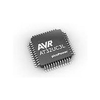
AT32UC3L032-D3UR Atmel, AT32UC3L032-D3UR Datasheet - Page 380

AT32UC3L032-D3UR
Manufacturer Part Number
AT32UC3L032-D3UR
Description
MCU AVR32 32KB FLASH 48TLLGA
Manufacturer
Atmel
Series
AVR®32 UC3r
Datasheet
1.AT32UC3L-EK.pdf
(858 pages)
Specifications of AT32UC3L032-D3UR
Core Processor
AVR
Core Size
32-Bit
Speed
50MHz
Connectivity
I²C, SPI, UART/USART
Peripherals
Brown-out Detect/Reset, DMA, PWM, WDT
Number Of I /o
36
Program Memory Size
32KB (32K x 8)
Program Memory Type
FLASH
Ram Size
16K x 8
Voltage - Supply (vcc/vdd)
1.62 V ~ 3.6 V
Data Converters
A/D 9x10b
Oscillator Type
Internal
Operating Temperature
-40°C ~ 85°C
Package / Case
48-TLLGA
Processor Series
AT32UC3x
Core
AVR32
Data Bus Width
32 bit
Data Ram Size
16 KB
Interface Type
SPI, TWI, USART
Maximum Clock Frequency
50 MHz
Number Of Programmable I/os
36
Number Of Timers
7
Maximum Operating Temperature
+ 85 C
Mounting Style
SMD/SMT
3rd Party Development Tools
EWAVR32, EWAVR32-BL
Development Tools By Supplier
AT32UC3L-EK
Minimum Operating Temperature
- 40 C
On-chip Adc
10 bit, 9 Channel
Lead Free Status / RoHS Status
Lead free / RoHS Compliant
Eeprom Size
-
Lead Free Status / Rohs Status
Details
- Current page: 380 of 858
- Download datasheet (13Mb)
19.6.4.4
19.6.4.5
19.6.4.6
19.6.4.7
32099F–11/2010
Receiver and Transmitter Control
Character Transmission
Character Reception
Receiver Timeout
See Section “19.6.2” on page 365.
The characters are sent by writing in the Transmit Holding Register (THR). The transmitter
reports two status bits in the Channel Status Register (CSR): TXRDY (Transmitter Ready),
which indicates that THR is empty and TXEMPTY, which indicates that all the characters written
in THR have been processed. When the current character processing is completed, the last
character written in THR is transferred into the Shift Register of the transmitter and THR
becomes empty, thus TXRDY rises.
Both TXRDY and TXEMPTY bits are low when the transmitter is disabled. Writing a character in
THR while TXRDY is low has no effect and the written character is lost.
If the USART is in SPI Slave Mode and if a character must be sent while the Transmit Holding
Register (THR) is empty, the UNRE (Underrun Error) bit is set. The TXD transmission line stays
at high level during all this time. The UNRE bit is cleared by writing the Control Register (CR)
with the RSTSTA (Reset Status) bit at 1.
In SPI Master Mode, the slave select line (NSS) is asserted at low level 1 Tbit before the trans-
mission of the MSB bit and released at high level 1 Tbit after the transmission of the LSB bit. So,
the slave select line (NSS) is always released between each character transmission and a mini-
mum delay of 3 Tbits always inserted. However, in order to address slave devices supporting the
CSAAT mode (Chip Select Active After Transfer), the slave select line (NSS) can be forced at
low level by writing the Control Register (CR) with the RTSEN bit at 1. The slave select line
(NSS) can be released at high level only by writing the Control Register (CR) with the RTSDIS
bit at 1 (for example, when all data have been transferred to the slave device).
In SPI Slave Mode, the transmitter does not require a falling edge of the slave select line (NSS)
to initiate a character transmission but only a low level. However, this low level must be present
on the slave select line (NSS) at least 1 Tbit before the first serial clock cycle corresponding to
the MSB bit.
When a character reception is completed, it is transferred to the Receive Holding Register
(RHR) and the RXRDY bit in the Status Register (CSR) rises. If a character is completed while
RXRDY is set, the OVRE (Overrun Error) bit is set. The last character is transferred into RHR
and overwrites the previous one. The OVRE bit is cleared by writing the Control Register (CR)
with the RSTSTA (Reset Status) bit at 1.
To ensure correct behavior of the receiver in SPI Slave Mode, the master device sending the
frame must ensure a minimum delay of 1 Tbit between each character transmission. The
receiver does not require a falling edge of the slave select line (NSS) to initiate a character
reception but only a low level. However, this low level must be present on the slave select line
(NSS) at least 1 Tbit before the first serial clock cycle corresponding to the MSB bit.
Because the receiver baudrate clock is active only during data transfers in SPI Mode, a receiver
timeout is impossible in this mode, whatever the Time-out value is (field TO) in the Time-out
Register (RTOR).
AT32UC3L016/32/64
380
Related parts for AT32UC3L032-D3UR
Image
Part Number
Description
Manufacturer
Datasheet
Request
R

Part Number:
Description:
KIT DEV/EVAL FOR AT32UC3L0
Manufacturer:
Atmel
Datasheet:

Part Number:
Description:
DEV KIT FOR AVR/AVR32
Manufacturer:
Atmel
Datasheet:

Part Number:
Description:
INTERVAL AND WIPE/WASH WIPER CONTROL IC WITH DELAY
Manufacturer:
ATMEL Corporation
Datasheet:

Part Number:
Description:
Low-Voltage Voice-Switched IC for Hands-Free Operation
Manufacturer:
ATMEL Corporation
Datasheet:

Part Number:
Description:
MONOLITHIC INTEGRATED FEATUREPHONE CIRCUIT
Manufacturer:
ATMEL Corporation
Datasheet:

Part Number:
Description:
AM-FM Receiver IC U4255BM-M
Manufacturer:
ATMEL Corporation
Datasheet:

Part Number:
Description:
Monolithic Integrated Feature Phone Circuit
Manufacturer:
ATMEL Corporation
Datasheet:

Part Number:
Description:
Multistandard Video-IF and Quasi Parallel Sound Processing
Manufacturer:
ATMEL Corporation
Datasheet:

Part Number:
Description:
High-performance EE PLD
Manufacturer:
ATMEL Corporation
Datasheet:

Part Number:
Description:
8-bit Flash Microcontroller
Manufacturer:
ATMEL Corporation
Datasheet:

Part Number:
Description:
2-Wire Serial EEPROM
Manufacturer:
ATMEL Corporation
Datasheet:


