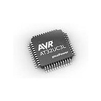
AT32UC3L032-D3UR Atmel, AT32UC3L032-D3UR Datasheet - Page 602

AT32UC3L032-D3UR
Manufacturer Part Number
AT32UC3L032-D3UR
Description
MCU AVR32 32KB FLASH 48TLLGA
Manufacturer
Atmel
Series
AVR®32 UC3r
Datasheet
1.AT32UC3L-EK.pdf
(858 pages)
Specifications of AT32UC3L032-D3UR
Core Processor
AVR
Core Size
32-Bit
Speed
50MHz
Connectivity
I²C, SPI, UART/USART
Peripherals
Brown-out Detect/Reset, DMA, PWM, WDT
Number Of I /o
36
Program Memory Size
32KB (32K x 8)
Program Memory Type
FLASH
Ram Size
16K x 8
Voltage - Supply (vcc/vdd)
1.62 V ~ 3.6 V
Data Converters
A/D 9x10b
Oscillator Type
Internal
Operating Temperature
-40°C ~ 85°C
Package / Case
48-TLLGA
Processor Series
AT32UC3x
Core
AVR32
Data Bus Width
32 bit
Data Ram Size
16 KB
Interface Type
SPI, TWI, USART
Maximum Clock Frequency
50 MHz
Number Of Programmable I/os
36
Number Of Timers
7
Maximum Operating Temperature
+ 85 C
Mounting Style
SMD/SMT
3rd Party Development Tools
EWAVR32, EWAVR32-BL
Development Tools By Supplier
AT32UC3L-EK
Minimum Operating Temperature
- 40 C
On-chip Adc
10 bit, 9 Channel
Lead Free Status / RoHS Status
Lead free / RoHS Compliant
Eeprom Size
-
Lead Free Status / Rohs Status
Details
- Current page: 602 of 858
- Download datasheet (13Mb)
26.5.4
26.5.5
26.5.6
26.6
26.6.1
26.6.2
32099F–11/2010
Functional Description
Interrupts
Peripheral Events
Debug Operation
Initializing the ADCIFB
Basic Operation
The ADCIFB interrupt request line is connected to the interrupt controller. Using the ADCIFB
interrupt request functionality requires the interrupt controller to be programmed first.
The ADCIFB peripheral events are connected via the Peripheral Event System. Refer to the
Peripheral Event System chapter for details
When an external debugger forces the CPU into debug mode, this module continues normal
operation. If this module is configured in a way that requires it to be periodically serviced by the
CPU through interrupt requests or similar, improper operation or data loss may result during
debugging.
The ADCIFB embeds a Successive Approximation Register (SAR) Analog-to-Digital Converter
(ADC). The ADC supports 8-bit or 10-bit resolution, which can be extended to 11 or 12 bits by
the Enhanced Resolution Mode.
The conversion is performed on a full range between 0 V and the reference voltage pin
ADVREFP. Analog inputs between these voltages converts to digital values (codes) based on a
linear conversion. This linear conversion is described in the expression below where M is the
number of bits used to represent the analog value, Vin is the voltage of the analog value to con-
vert, Vref is the maximum voltage, and Code is the converted digital value.
The ADC Interface is enabled by writing a one to the Enable bit in the Control Register (CR.EN).
After the ADC Interface is enabled, the ADC timings needs to be configured by writing the cor-
rect values to the RES, PRESCAL, and STARTUP fields in the ADC Configuration Register
(ACR). See
I/O Controller must be configured correctly and the Reference Voltage (ADVREFP) signal must
be connected. Refer to
To convert analog values to digital values the user must first initialize the ADCIFB as described
in
writing a one the corresponding bits in the Channel Enable Register (CHER). Enabling channel
N instructs the ADCIFB to convert the analog voltage applied to AD pin N at each conversion
sequence. Multiple channels can be enabled resulting in multiple AD pins being converted at
each conversion sequence.
To start converting data the user can either manually start a conversion sequence by writing a
one to the START bit in the Control Register (CR.START) or configure an automatic trigger to
initiate the conversions. The automatic trigger can be configured to trig on many different condi-
tions. Refer to
Section
26.6.1. When the ADCIFB is initialized the channels to convert must be enabled by
Section
Section 26.8.1
26.6.6, and
Section 26.5.1
for details.
Section 26.6.8
for details.
Code
=
for details. Before the ADCIFB can be used, the
2
------------------- -
M
V
⋅
ref
V
in
AT32UC3L016/32/64
602
Related parts for AT32UC3L032-D3UR
Image
Part Number
Description
Manufacturer
Datasheet
Request
R

Part Number:
Description:
KIT DEV/EVAL FOR AT32UC3L0
Manufacturer:
Atmel
Datasheet:

Part Number:
Description:
DEV KIT FOR AVR/AVR32
Manufacturer:
Atmel
Datasheet:

Part Number:
Description:
INTERVAL AND WIPE/WASH WIPER CONTROL IC WITH DELAY
Manufacturer:
ATMEL Corporation
Datasheet:

Part Number:
Description:
Low-Voltage Voice-Switched IC for Hands-Free Operation
Manufacturer:
ATMEL Corporation
Datasheet:

Part Number:
Description:
MONOLITHIC INTEGRATED FEATUREPHONE CIRCUIT
Manufacturer:
ATMEL Corporation
Datasheet:

Part Number:
Description:
AM-FM Receiver IC U4255BM-M
Manufacturer:
ATMEL Corporation
Datasheet:

Part Number:
Description:
Monolithic Integrated Feature Phone Circuit
Manufacturer:
ATMEL Corporation
Datasheet:

Part Number:
Description:
Multistandard Video-IF and Quasi Parallel Sound Processing
Manufacturer:
ATMEL Corporation
Datasheet:

Part Number:
Description:
High-performance EE PLD
Manufacturer:
ATMEL Corporation
Datasheet:

Part Number:
Description:
8-bit Flash Microcontroller
Manufacturer:
ATMEL Corporation
Datasheet:

Part Number:
Description:
2-Wire Serial EEPROM
Manufacturer:
ATMEL Corporation
Datasheet:


