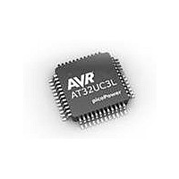
AT32UC3L032-D3UR Atmel, AT32UC3L032-D3UR Datasheet - Page 610

AT32UC3L032-D3UR
Manufacturer Part Number
AT32UC3L032-D3UR
Description
MCU AVR32 32KB FLASH 48TLLGA
Manufacturer
Atmel
Series
AVR®32 UC3r
Datasheet
1.AT32UC3L-EK.pdf
(858 pages)
Specifications of AT32UC3L032-D3UR
Core Processor
AVR
Core Size
32-Bit
Speed
50MHz
Connectivity
I²C, SPI, UART/USART
Peripherals
Brown-out Detect/Reset, DMA, PWM, WDT
Number Of I /o
36
Program Memory Size
32KB (32K x 8)
Program Memory Type
FLASH
Ram Size
16K x 8
Voltage - Supply (vcc/vdd)
1.62 V ~ 3.6 V
Data Converters
A/D 9x10b
Oscillator Type
Internal
Operating Temperature
-40°C ~ 85°C
Package / Case
48-TLLGA
Processor Series
AT32UC3x
Core
AVR32
Data Bus Width
32 bit
Data Ram Size
16 KB
Interface Type
SPI, TWI, USART
Maximum Clock Frequency
50 MHz
Number Of Programmable I/os
36
Number Of Timers
7
Maximum Operating Temperature
+ 85 C
Mounting Style
SMD/SMT
3rd Party Development Tools
EWAVR32, EWAVR32-BL
Development Tools By Supplier
AT32UC3L-EK
Minimum Operating Temperature
- 40 C
On-chip Adc
10 bit, 9 Channel
Lead Free Status / RoHS Status
Lead free / RoHS Compliant
Eeprom Size
-
Lead Free Status / Rohs Status
Details
- Current page: 610 of 858
- Download datasheet (13Mb)
26.7.4
32099F–11/2010
Resistive Touch Screen Sequencer
Figure 26-3. Resistive Touch Screen Pin Connections
The Resistive Touch Screen Sequencer is responsible for applying voltage to the resistive touch
screen films as described in
output value of the ADP and AD pins. This allows the Resistive Touch Screen Sequencer to add
a voltage gradient on one film while keeping the other film floating so a touch can be measured.
The Resistive Touch Screen Sequencer will when measuring the vertical position, apply VDD
and GND to the pins connected to X
measurement of Y
non ideal pad drivers, the actual voltage of X
VDD and GND can be used in the contact point calculation to increase accuracy. See second
formula in
When the vertical values are converted the same setup is applies for the second axes, by setting
X
details.
P
and X
M
Section
in tristate mode and applying VDD and GND to Y
Analog Pin Output Enable (MR.APOE) == 1
Analog Pin Output Enable (MR.APOE) == 0
P
26.7.2.
can proceed without interference. To compensate for ADC offset errors and
Y
Y
M
M
X
X
Section
M
M
P
26.7.2. This is done by controlling the output enable and the
and X
M
X
P
X
. The Y
P
P
and X
Y
Y
P
P
P
M
and Y
is measured as well, so the real values for
AT32UC3L016/32/64
M
P
and Y
pins are put in tristate mode so the
NC
NC
AD
AD
AD
AD
AD
M
AD
AD
AD
DP
DP
DP
DP
. Refer to
tspo+0
tspo+3
tspo+0
tspo+3
tspo+1
tspo+1
tspo+2
tspo+2
0
1
0
1
Section 26.8.3
610
for
Related parts for AT32UC3L032-D3UR
Image
Part Number
Description
Manufacturer
Datasheet
Request
R

Part Number:
Description:
KIT DEV/EVAL FOR AT32UC3L0
Manufacturer:
Atmel
Datasheet:

Part Number:
Description:
DEV KIT FOR AVR/AVR32
Manufacturer:
Atmel
Datasheet:

Part Number:
Description:
INTERVAL AND WIPE/WASH WIPER CONTROL IC WITH DELAY
Manufacturer:
ATMEL Corporation
Datasheet:

Part Number:
Description:
Low-Voltage Voice-Switched IC for Hands-Free Operation
Manufacturer:
ATMEL Corporation
Datasheet:

Part Number:
Description:
MONOLITHIC INTEGRATED FEATUREPHONE CIRCUIT
Manufacturer:
ATMEL Corporation
Datasheet:

Part Number:
Description:
AM-FM Receiver IC U4255BM-M
Manufacturer:
ATMEL Corporation
Datasheet:

Part Number:
Description:
Monolithic Integrated Feature Phone Circuit
Manufacturer:
ATMEL Corporation
Datasheet:

Part Number:
Description:
Multistandard Video-IF and Quasi Parallel Sound Processing
Manufacturer:
ATMEL Corporation
Datasheet:

Part Number:
Description:
High-performance EE PLD
Manufacturer:
ATMEL Corporation
Datasheet:

Part Number:
Description:
8-bit Flash Microcontroller
Manufacturer:
ATMEL Corporation
Datasheet:

Part Number:
Description:
2-Wire Serial EEPROM
Manufacturer:
ATMEL Corporation
Datasheet:


