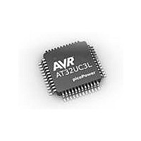
AT32UC3L032-D3UR Atmel, AT32UC3L032-D3UR Datasheet - Page 429

AT32UC3L032-D3UR
Manufacturer Part Number
AT32UC3L032-D3UR
Description
MCU AVR32 32KB FLASH 48TLLGA
Manufacturer
Atmel
Series
AVR®32 UC3r
Datasheet
1.AT32UC3L-EK.pdf
(858 pages)
Specifications of AT32UC3L032-D3UR
Core Processor
AVR
Core Size
32-Bit
Speed
50MHz
Connectivity
I²C, SPI, UART/USART
Peripherals
Brown-out Detect/Reset, DMA, PWM, WDT
Number Of I /o
36
Program Memory Size
32KB (32K x 8)
Program Memory Type
FLASH
Ram Size
16K x 8
Voltage - Supply (vcc/vdd)
1.62 V ~ 3.6 V
Data Converters
A/D 9x10b
Oscillator Type
Internal
Operating Temperature
-40°C ~ 85°C
Package / Case
48-TLLGA
Processor Series
AT32UC3x
Core
AVR32
Data Bus Width
32 bit
Data Ram Size
16 KB
Interface Type
SPI, TWI, USART
Maximum Clock Frequency
50 MHz
Number Of Programmable I/os
36
Number Of Timers
7
Maximum Operating Temperature
+ 85 C
Mounting Style
SMD/SMT
3rd Party Development Tools
EWAVR32, EWAVR32-BL
Development Tools By Supplier
AT32UC3L-EK
Minimum Operating Temperature
- 40 C
On-chip Adc
10 bit, 9 Channel
Lead Free Status / RoHS Status
Lead free / RoHS Compliant
Eeprom Size
-
Lead Free Status / Rohs Status
Details
- Current page: 429 of 858
- Download datasheet (13Mb)
20.7.2
Figure 20-3. SPI Transfer Format (NCPHA = 1, 8 bits per transfer)
32099F–11/2010
SPCK cycle (for reference)
Data Transfer
(from master)
(from slave)
(CPOL = 0)
(CPOL = 1)
(to slave)
SPCK
SPCK
MOSI
MISO
NSS
Four combinations of polarity and phase are available for data transfers. The clock polarity is
configured with the Clock Polarity bit in the Chip Select Registers (CSRn.CPOL). The clock
phase is configured with the Clock Phase bit in the CSRn registers (CSRn.NCPHA). These two
bits determine the edges of the clock signal on which data is driven and sampled. Each of the
two bits has two possible states, resulting in four possible combinations that are incompatible
with one another. Thus, a master/slave pair must use the same parameter pair values to com-
municate. If multiple slaves are used and fixed in different configurations, the master must
reconfigure itself each time it needs to communicate with a different slave.
Table 20-2 on page 429
Table 20-2.
Figure 20-3 on page 429
MSB
1
MSB
*** Not Defined, but normaly MSB of previous character received
SPI modes
2
6
6
SPI Mode
0
1
2
3
3
shows the four modes and corresponding parameter settings.
and
5
5
Figure 20-4 on page 430
4
4
4
5
3
3
6
2
2
show examples of data transfers.
7
AT32UC3L016/32/64
CPOL
1
1
0
0
1
1
8
LSB
LSB
***
NCPHA
1
0
1
0
429
Related parts for AT32UC3L032-D3UR
Image
Part Number
Description
Manufacturer
Datasheet
Request
R

Part Number:
Description:
KIT DEV/EVAL FOR AT32UC3L0
Manufacturer:
Atmel
Datasheet:

Part Number:
Description:
DEV KIT FOR AVR/AVR32
Manufacturer:
Atmel
Datasheet:

Part Number:
Description:
INTERVAL AND WIPE/WASH WIPER CONTROL IC WITH DELAY
Manufacturer:
ATMEL Corporation
Datasheet:

Part Number:
Description:
Low-Voltage Voice-Switched IC for Hands-Free Operation
Manufacturer:
ATMEL Corporation
Datasheet:

Part Number:
Description:
MONOLITHIC INTEGRATED FEATUREPHONE CIRCUIT
Manufacturer:
ATMEL Corporation
Datasheet:

Part Number:
Description:
AM-FM Receiver IC U4255BM-M
Manufacturer:
ATMEL Corporation
Datasheet:

Part Number:
Description:
Monolithic Integrated Feature Phone Circuit
Manufacturer:
ATMEL Corporation
Datasheet:

Part Number:
Description:
Multistandard Video-IF and Quasi Parallel Sound Processing
Manufacturer:
ATMEL Corporation
Datasheet:

Part Number:
Description:
High-performance EE PLD
Manufacturer:
ATMEL Corporation
Datasheet:

Part Number:
Description:
8-bit Flash Microcontroller
Manufacturer:
ATMEL Corporation
Datasheet:

Part Number:
Description:
2-Wire Serial EEPROM
Manufacturer:
ATMEL Corporation
Datasheet:


