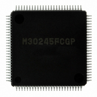
M30245FCGP#U1 Renesas Electronics America, M30245FCGP#U1 Datasheet - Page 11

M30245FCGP#U1
Manufacturer Part Number
M30245FCGP#U1
Description
IC M16C/24 MCU FLSH 128K 100LQFP
Manufacturer
Renesas Electronics America
Series
M16C™ M16C/20r
Datasheet
1.M30245FCGPU1.pdf
(268 pages)
Specifications of M30245FCGP#U1
Core Processor
M16C/60
Core Size
16-Bit
Speed
16MHz
Connectivity
I²C, SPI, SSI, UART/USART, USB
Peripherals
DMA, PWM, WDT
Number Of I /o
82
Program Memory Size
128KB (128K x 8)
Program Memory Type
FLASH
Ram Size
10K x 8
Voltage - Supply (vcc/vdd)
3 V ~ 3.6 V
Data Converters
A/D 8x10b
Oscillator Type
Internal
Operating Temperature
-20°C ~ 85°C
Package / Case
100-LQFP
Package
100LQFP
Family Name
R8C
Maximum Speed
16 MHz
Operating Supply Voltage
3.3 V
Data Bus Width
16 Bit
Number Of Programmable I/os
82
Interface Type
USB/UART/I2C/SPI
On-chip Adc
8-chx10-bit
Number Of Timers
5
Lead Free Status / RoHS Status
Lead free / RoHS Compliant
Eeprom Size
-
Available stocks
Company
Part Number
Manufacturer
Quantity
Price
- Current page: 11 of 268
- Download datasheet (3Mb)
M30245 Group
Table 1.3
Rev.2.00
REJ03B0005-0200
Port
P10
P9
P6
P7
P8
I/O port
UART/SSI
I/
Timer A
UART
LED drive
I/O port
I/O port
A/D
USB-ATTACH
USB SOF
I/O port
Key-input interrupt
Analog input
External interrupt input
Input
Sub-Clock
O port
Pin description
Oct 16, 2006
Function
page 9 of 264
P6
CTS/RTS/SS/WS
CLK/SCK
RxD/SCL/STxD/RX
TxD/SDA/SRxD/XMT
P7
TA
TA
CTS/RTS/SS/WS
CLK/SCK
RxD/SCL/STxD
TxD/SDA/SRxD
LED
P8
P9
AD
ATTACH
SOF
P10
KI
AN
INT0 to INT2
P8
XC
0
OUT
IN
0
0
0
0
5
TRG
0
IN
to KI
, P9
/NMI
0
Pin Name
to P6
to P7
0
to P8
to AN
, XC
to P10
to LED
2
7
, P9
OUT
7
7
4
7
, P8
7
3
7
6
, P8
7
I/O
I/O
I/O
I/O
I/O
I, O
I/O
I/O
I/O
O
O
O
O
I
I
I
I
I
I
This is an 8-bit I/O port equivalent to P0.
P6
P6
These pins can be used for Serial Sound Interface, I
This is an 8-bit I/O port equivalent to P0. P7
output.
P7
P7
These pins can be used for I
These pins are capable of sinking 20mA for driving LEDs.
This is a 7-bit I/O port equivalent to P0.
P8
This is a 3-bit I/O port equivalent to P0.
P9
USB cable.
P92 is an output for the USB start of frame signal pulse.
This is an 8-bit I/O port equivalent to P0.
P7
P8
Input port for NMI interrupt.
P9
P10
P10
0
4
0
0
4
6
0
2
3
0
0
to P6
to P6
to P7
to P7
to P7
and P8
can be used to attach or detach from the USB host without disconnecting the
to P8
is an A/D trigger input port.
to P10
to P10
3
7
7
3
7
4
are I/O ports for UART0.
are I/O ports for UART1.
are I/O ports for UART2.
are I/O ports for UART3.
are I/O ports for Timer A0 to A3.
are external interrupt input ports.
7
7
7
, connect an oscillator between these pins for sub-clock generation.
are key-input interrupt ports.
are analog input ports for A/D converter.
2
C and SPI communication.
Description
0
and P7
2
1
C and SPI communication.
are N-channel open drain
Description
Related parts for M30245FCGP#U1
Image
Part Number
Description
Manufacturer
Datasheet
Request
R

Part Number:
Description:
KIT STARTER FOR M16C/29
Manufacturer:
Renesas Electronics America
Datasheet:

Part Number:
Description:
KIT STARTER FOR R8C/2D
Manufacturer:
Renesas Electronics America
Datasheet:

Part Number:
Description:
R0K33062P STARTER KIT
Manufacturer:
Renesas Electronics America
Datasheet:

Part Number:
Description:
KIT STARTER FOR R8C/23 E8A
Manufacturer:
Renesas Electronics America
Datasheet:

Part Number:
Description:
KIT STARTER FOR R8C/25
Manufacturer:
Renesas Electronics America
Datasheet:

Part Number:
Description:
KIT STARTER H8S2456 SHARPE DSPLY
Manufacturer:
Renesas Electronics America
Datasheet:

Part Number:
Description:
KIT STARTER FOR R8C38C
Manufacturer:
Renesas Electronics America
Datasheet:

Part Number:
Description:
KIT STARTER FOR R8C35C
Manufacturer:
Renesas Electronics America
Datasheet:

Part Number:
Description:
KIT STARTER FOR R8CL3AC+LCD APPS
Manufacturer:
Renesas Electronics America
Datasheet:

Part Number:
Description:
KIT STARTER FOR RX610
Manufacturer:
Renesas Electronics America
Datasheet:

Part Number:
Description:
KIT STARTER FOR R32C/118
Manufacturer:
Renesas Electronics America
Datasheet:

Part Number:
Description:
KIT DEV RSK-R8C/26-29
Manufacturer:
Renesas Electronics America
Datasheet:

Part Number:
Description:
KIT STARTER FOR SH7124
Manufacturer:
Renesas Electronics America
Datasheet:

Part Number:
Description:
KIT STARTER FOR H8SX/1622
Manufacturer:
Renesas Electronics America
Datasheet:


