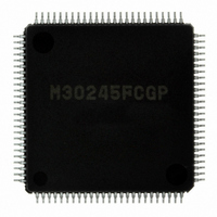
M30245FCGP#U1 Renesas Electronics America, M30245FCGP#U1 Datasheet - Page 32

M30245FCGP#U1
Manufacturer Part Number
M30245FCGP#U1
Description
IC M16C/24 MCU FLSH 128K 100LQFP
Manufacturer
Renesas Electronics America
Series
M16C™ M16C/20r
Datasheet
1.M30245FCGPU1.pdf
(268 pages)
Specifications of M30245FCGP#U1
Core Processor
M16C/60
Core Size
16-Bit
Speed
16MHz
Connectivity
I²C, SPI, SSI, UART/USART, USB
Peripherals
DMA, PWM, WDT
Number Of I /o
82
Program Memory Size
128KB (128K x 8)
Program Memory Type
FLASH
Ram Size
10K x 8
Voltage - Supply (vcc/vdd)
3 V ~ 3.6 V
Data Converters
A/D 8x10b
Oscillator Type
Internal
Operating Temperature
-20°C ~ 85°C
Package / Case
100-LQFP
Package
100LQFP
Family Name
R8C
Maximum Speed
16 MHz
Operating Supply Voltage
3.3 V
Data Bus Width
16 Bit
Number Of Programmable I/os
82
Interface Type
USB/UART/I2C/SPI
On-chip Adc
8-chx10-bit
Number Of Timers
5
Lead Free Status / RoHS Status
Lead free / RoHS Compliant
Eeprom Size
-
Available stocks
Company
Part Number
Manufacturer
Quantity
Price
- Current page: 32 of 268
- Download datasheet (3Mb)
M30245 Group
Rev.2.00
REJ03B0005-0200
Figure 1.13. Chip-select control register
Bus Control
The following explains the signals required for accessing external devices and software waits. The signals
required for accessing the external devices are valid when the processor mode is set to memory expansion
mode and microprocessor mode. The software waits are valid in all processor modes.
Oct 16, 2006
Address bus/data bus
Chip select signal
The address bus consists of the 20 pins A
The data bus consists of the pins for data I/O. When the BYTE pin is "H", the 8 ports (D
bus. When BYTE is "L", the 16 ports (D
When a change is made from single-chip mode to memory expansion mode, the value of the address bus is
undefined until external memory is accessed.
The chip select signal is output using the same pins as P4
(address 0008
register is valid in memory expansion mode and microprocessor mode. In single-chip mode, P4
function as programmable I/O ports regardless of the value in the chip select control register.
In microprocessor mode, only CS0 outputs the chip select signal after reset. CS1 to CS3 function as input ports.
Figure 1.13 shows the chip select control register.
The chip select signal can be used to split the external area into as many as four blocks. Table 1.16 shows the
external memory areas specified using the chip select signal.
Chip select control register
Chip select expansion register
b7
b7
b6
b6
b5 b4
b5 b4
page 30 of 264
16
b3 b2
b3 b2
) set each pin to function as an I/O port or to output the chip select signal. The chip select control
b1
b1
b0
b0
Note :Set CSEiW bits (i = 0 to 3) after setting the corresponding CSiW bit (i = 0 to 3) of the CSR register
Bit Symbol
Bit Symbol
CS0
CS1
CS2
CS3
CS0W
CS1W
CS2W
CS3W
CSE0W
CSE1W
CSE2W
CSE3W
Symbol
CSR
Symbol
CSE
to "0". When CSiW bits are set to "1", CSEiW bits must be returned to "00
CS0 output enable bit
CS1 output enable bit
CS2 output enable bit
CS3 output enable bit
CS0wait bit
CS1wait bit
CS2wait bit
CS3wait bit
CS0wait expansion bit
CS1wait expansion bit
CS2wait expansion bit
CS3wait expansion bit
0
Bit Name
to D
0
Bit Name
to A
15)
19
function as the data bus.
for accessing the 1M bytes of address space.
0 : Chip select output disabled (Normal port pin)
1 : Chip select output enabled
0 : Wait state inserted
1 : No wait state
Address
Address
0008
001B
4
to P4
16
16
0 0 : 1 Wait state
0 1 : 2 Wait states
1 0 : 3 Wait states
1 1 : Inhibited
7
. Bits 0 to 3 of the chip select control register
Function
Function
2
".
When reset
When reset
01
00
0
16
16
to D
O
O
O
O
O
O
O
R
O
Processor Mode
7)
O
O
O
R
O
function as the data
O
O
O
O
O
W
O
O
O
W
O
O
O
O
4
to P4
7
Related parts for M30245FCGP#U1
Image
Part Number
Description
Manufacturer
Datasheet
Request
R

Part Number:
Description:
KIT STARTER FOR M16C/29
Manufacturer:
Renesas Electronics America
Datasheet:

Part Number:
Description:
KIT STARTER FOR R8C/2D
Manufacturer:
Renesas Electronics America
Datasheet:

Part Number:
Description:
R0K33062P STARTER KIT
Manufacturer:
Renesas Electronics America
Datasheet:

Part Number:
Description:
KIT STARTER FOR R8C/23 E8A
Manufacturer:
Renesas Electronics America
Datasheet:

Part Number:
Description:
KIT STARTER FOR R8C/25
Manufacturer:
Renesas Electronics America
Datasheet:

Part Number:
Description:
KIT STARTER H8S2456 SHARPE DSPLY
Manufacturer:
Renesas Electronics America
Datasheet:

Part Number:
Description:
KIT STARTER FOR R8C38C
Manufacturer:
Renesas Electronics America
Datasheet:

Part Number:
Description:
KIT STARTER FOR R8C35C
Manufacturer:
Renesas Electronics America
Datasheet:

Part Number:
Description:
KIT STARTER FOR R8CL3AC+LCD APPS
Manufacturer:
Renesas Electronics America
Datasheet:

Part Number:
Description:
KIT STARTER FOR RX610
Manufacturer:
Renesas Electronics America
Datasheet:

Part Number:
Description:
KIT STARTER FOR R32C/118
Manufacturer:
Renesas Electronics America
Datasheet:

Part Number:
Description:
KIT DEV RSK-R8C/26-29
Manufacturer:
Renesas Electronics America
Datasheet:

Part Number:
Description:
KIT STARTER FOR SH7124
Manufacturer:
Renesas Electronics America
Datasheet:

Part Number:
Description:
KIT STARTER FOR H8SX/1622
Manufacturer:
Renesas Electronics America
Datasheet:


