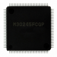
M30245FCGP#U1 Renesas Electronics America, M30245FCGP#U1 Datasheet - Page 164

M30245FCGP#U1
Manufacturer Part Number
M30245FCGP#U1
Description
IC M16C/24 MCU FLSH 128K 100LQFP
Manufacturer
Renesas Electronics America
Series
M16C™ M16C/20r
Datasheet
1.M30245FCGPU1.pdf
(268 pages)
Specifications of M30245FCGP#U1
Core Processor
M16C/60
Core Size
16-Bit
Speed
16MHz
Connectivity
I²C, SPI, SSI, UART/USART, USB
Peripherals
DMA, PWM, WDT
Number Of I /o
82
Program Memory Size
128KB (128K x 8)
Program Memory Type
FLASH
Ram Size
10K x 8
Voltage - Supply (vcc/vdd)
3 V ~ 3.6 V
Data Converters
A/D 8x10b
Oscillator Type
Internal
Operating Temperature
-20°C ~ 85°C
Package / Case
100-LQFP
Package
100LQFP
Family Name
R8C
Maximum Speed
16 MHz
Operating Supply Voltage
3.3 V
Data Bus Width
16 Bit
Number Of Programmable I/os
82
Interface Type
USB/UART/I2C/SPI
On-chip Adc
8-chx10-bit
Number Of Timers
5
Lead Free Status / RoHS Status
Lead free / RoHS Compliant
Eeprom Size
-
Available stocks
Company
Part Number
Manufacturer
Quantity
Price
- Current page: 164 of 268
- Download datasheet (3Mb)
M30245 Group
Figure 1.121. Serial Sound Interface related registers (1)
Rev.2.00
REJ03B0005-0200
The data interface for the receiver behaves slightly different for the same case. When the receive shift register loads
data into the left buffer, the state machine generates an interrupt. A word read from the MCU causes 16 bits to be
read. The other 8 bits are latched into a temporary buffer. Latching the data into a temporary buffer empties the left
buffer that provides additional time for the MCU to read the data without an overflow condition occurring. Even though
there are unread bits, no interrupt is generated because a word read would read a byte from the right buffer which
would be invalid data. The data in the right buffer is from the previous receive cycle and therefore invalid for the read
cycle. Thus, the complete read of the left buffer is delayed until the right buffer is loaded by the receive shift register
and the receive interrupts should be assigned higher priority than transmit if the Serial Sound Interface is set up for
both transmit and receive.
The Serial Sound Interface also contains a rate feedback mechanism which can be used to determine the rate of
data transfer via the Serial Sound Interface relative to the USB. It consists of a 16-bit counter with either SCK or WS
as the count source and a 16-bit register to store the count value. The count value is loaded into the register on each
negative edge of SOF pulse generated by the USB core. The counter is also reset by the SOF pulse. The SOF pulse
is a frame delimiter used in USB communication. Refer to the USB section for details. The value read from the
register is the count from the immediately preceding USB frame.
Figure 1.121 shows the Serial Sound Interface rate feedback registers and Serial Sound Interface transmit and
receive data buffer registers. Figure 1.122. shows the Serial Sound Interface mode registers.
Oct 16, 2006
Serial Sound Interface transmit buffer register
Serial Sound Interface receive buffer register
Serial Sound Interface rate feedback register
(b15
(b15
(b15
b7
b7
b7
b8)
b0 b7
b8)
b0 b7
b8)
b0
page 162 of 264
b7
b0
b0
b0
Note: Write only to even byte (8 bit) or entire word (16 bit).
Transmit data (Note)
Note: Read only from even byte (8 bit) or entire word (16 bit)
Receive data (Note)
Rate feedback counter value
Symbol
SSIiTXB (i = 0, 1)
Symbol
SSIiRXB (i = 0, 1)
Symbol
SSIiRF (i = 0, 1)
Function
Function
Function
0315
0317
0375
0377
0319
0379
Address
Address
Address
16
16,
16
16
16,
16,
, 0314
, 0316
, 0318
0374
0376
0378
16
16
16
16
16
16
Serial Sound Interface
When reset
When reset
0000
When reset
0000
0000
16
16
X
R W
O
O
R W
R W
16
O
X
X
Related parts for M30245FCGP#U1
Image
Part Number
Description
Manufacturer
Datasheet
Request
R

Part Number:
Description:
KIT STARTER FOR M16C/29
Manufacturer:
Renesas Electronics America
Datasheet:

Part Number:
Description:
KIT STARTER FOR R8C/2D
Manufacturer:
Renesas Electronics America
Datasheet:

Part Number:
Description:
R0K33062P STARTER KIT
Manufacturer:
Renesas Electronics America
Datasheet:

Part Number:
Description:
KIT STARTER FOR R8C/23 E8A
Manufacturer:
Renesas Electronics America
Datasheet:

Part Number:
Description:
KIT STARTER FOR R8C/25
Manufacturer:
Renesas Electronics America
Datasheet:

Part Number:
Description:
KIT STARTER H8S2456 SHARPE DSPLY
Manufacturer:
Renesas Electronics America
Datasheet:

Part Number:
Description:
KIT STARTER FOR R8C38C
Manufacturer:
Renesas Electronics America
Datasheet:

Part Number:
Description:
KIT STARTER FOR R8C35C
Manufacturer:
Renesas Electronics America
Datasheet:

Part Number:
Description:
KIT STARTER FOR R8CL3AC+LCD APPS
Manufacturer:
Renesas Electronics America
Datasheet:

Part Number:
Description:
KIT STARTER FOR RX610
Manufacturer:
Renesas Electronics America
Datasheet:

Part Number:
Description:
KIT STARTER FOR R32C/118
Manufacturer:
Renesas Electronics America
Datasheet:

Part Number:
Description:
KIT DEV RSK-R8C/26-29
Manufacturer:
Renesas Electronics America
Datasheet:

Part Number:
Description:
KIT STARTER FOR SH7124
Manufacturer:
Renesas Electronics America
Datasheet:

Part Number:
Description:
KIT STARTER FOR H8SX/1622
Manufacturer:
Renesas Electronics America
Datasheet:


