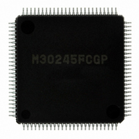
M30245FCGP#U1 Renesas Electronics America, M30245FCGP#U1 Datasheet - Page 253

M30245FCGP#U1
Manufacturer Part Number
M30245FCGP#U1
Description
IC M16C/24 MCU FLSH 128K 100LQFP
Manufacturer
Renesas Electronics America
Series
M16C™ M16C/20r
Datasheet
1.M30245FCGPU1.pdf
(268 pages)
Specifications of M30245FCGP#U1
Core Processor
M16C/60
Core Size
16-Bit
Speed
16MHz
Connectivity
I²C, SPI, SSI, UART/USART, USB
Peripherals
DMA, PWM, WDT
Number Of I /o
82
Program Memory Size
128KB (128K x 8)
Program Memory Type
FLASH
Ram Size
10K x 8
Voltage - Supply (vcc/vdd)
3 V ~ 3.6 V
Data Converters
A/D 8x10b
Oscillator Type
Internal
Operating Temperature
-20°C ~ 85°C
Package / Case
100-LQFP
Package
100LQFP
Family Name
R8C
Maximum Speed
16 MHz
Operating Supply Voltage
3.3 V
Data Bus Width
16 Bit
Number Of Programmable I/os
82
Interface Type
USB/UART/I2C/SPI
On-chip Adc
8-chx10-bit
Number Of Timers
5
Lead Free Status / RoHS Status
Lead free / RoHS Compliant
Eeprom Size
-
Available stocks
Company
Part Number
Manufacturer
Quantity
Price
- Current page: 253 of 268
- Download datasheet (3Mb)
M30245 Group
Rev.2.00
REJ03B0005-0200
Pulse modulation mode
A/D converter
Serial I/O (UART Mode)
The Timer Ai interrupt request bit becomes “1” if setting operation mode of the timer in compliance with any of the
following procedures:
• Selecting PWM mode after reset.
• Changing operation mode from timer mode to PWM mode.
• Changing operation mode from event counter mode to PWM mode.
Therefore, to use Timer Ai interrupt (interrupt request bit), set Timer Ai interrupt request bit to “0” after the above listed
changes have been made.
Setting the count start flag to “0” while PWM pulses are being output causes the counter to stop counting. If the TAi
pin is outputting an “H” level in this instance, the output level goes to “L”, and the Timer Ai interrupt request bit goes to
“1”. If the TAi
request bit does not becomes “1”.
• Write to each bit (except bit 6) of AD control register 0, AD control register 1, and to bit 0 of AD control register 2
when A/D conversion is stopped (before a trigger occurs). When the V
wait 1 µs or longer before starting A/D conversion.
• When changing A/D operation mode, select the analog input pin again.
• Using one-shot mode or single sweep mode:
Read the corresponding AD register after confirming A/D conversion is finished. (Check the A/D conversion interrupt
request bit.)
• Using repeat mode, repeat sweep mode 0 or repeat sweep mode 1:
Use the undivided main clock as the internal CPU clock.
When f(X
Description
Oct 16, 2006
in
) is faster than 10MHz, make the A/D frequency 10MHz or less by dividing.
OUT
When the CLKi and CTSi pin level goes to “H” (Note 1), if the UiMR register is set to either of the
following settings, the UiERE bit of the UiC1 register is set to “1” (parity error signal output enabled).
When the PRYE bit of the UiMR register is set to “1” while the UiERE bit is “1” (parity error signal output
enabled), if a parity error occurs at receiving data, the T
the UiERE bit after setting the UiMR register.
• Set bits SMD2 through SMD0 to “000
• Set bits SMD2 through SMD0 to “001
• Set bits SMD2 through SMD0 to “001
• Set bits SMD2 through SMD0 to “001
• Set bits SMD2 through SMD0 to “010
Note 1: If the pins are not used as CLKi or CTSi, these conditions apply when the pin level goes to “H”.
8 bits long)
mode transfer data 7 bits long)
mode transfer data 8 bits long)
long)
pin is outputting an “L” level in this instance, the level does not change, and the Timer Ai interrupt
page 251 of 264
2
2
2
2
2
” (clock synchronous serial I/O mode) through “100
” (clock synchronous serial I/O mode) through “101
” (I2C mode) through “101
” (serial I/O disabled) through “101
” (clock synchronous serial I/O mode) transfer data 9 bits long)
X
REF
Di pin outputs the “L” level. To prevent this, set
connection bit is changed from "0" to “1”,
2
” (UART mode transfer data 8 bits
2
” (UART mode transfer data
Usage Notes
2
2
” (UART
” (UART
OUT
Related parts for M30245FCGP#U1
Image
Part Number
Description
Manufacturer
Datasheet
Request
R

Part Number:
Description:
KIT STARTER FOR M16C/29
Manufacturer:
Renesas Electronics America
Datasheet:

Part Number:
Description:
KIT STARTER FOR R8C/2D
Manufacturer:
Renesas Electronics America
Datasheet:

Part Number:
Description:
R0K33062P STARTER KIT
Manufacturer:
Renesas Electronics America
Datasheet:

Part Number:
Description:
KIT STARTER FOR R8C/23 E8A
Manufacturer:
Renesas Electronics America
Datasheet:

Part Number:
Description:
KIT STARTER FOR R8C/25
Manufacturer:
Renesas Electronics America
Datasheet:

Part Number:
Description:
KIT STARTER H8S2456 SHARPE DSPLY
Manufacturer:
Renesas Electronics America
Datasheet:

Part Number:
Description:
KIT STARTER FOR R8C38C
Manufacturer:
Renesas Electronics America
Datasheet:

Part Number:
Description:
KIT STARTER FOR R8C35C
Manufacturer:
Renesas Electronics America
Datasheet:

Part Number:
Description:
KIT STARTER FOR R8CL3AC+LCD APPS
Manufacturer:
Renesas Electronics America
Datasheet:

Part Number:
Description:
KIT STARTER FOR RX610
Manufacturer:
Renesas Electronics America
Datasheet:

Part Number:
Description:
KIT STARTER FOR R32C/118
Manufacturer:
Renesas Electronics America
Datasheet:

Part Number:
Description:
KIT DEV RSK-R8C/26-29
Manufacturer:
Renesas Electronics America
Datasheet:

Part Number:
Description:
KIT STARTER FOR SH7124
Manufacturer:
Renesas Electronics America
Datasheet:

Part Number:
Description:
KIT STARTER FOR H8SX/1622
Manufacturer:
Renesas Electronics America
Datasheet:


