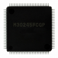
M30245FCGP#U1 Renesas Electronics America, M30245FCGP#U1 Datasheet - Page 264

M30245FCGP#U1
Manufacturer Part Number
M30245FCGP#U1
Description
IC M16C/24 MCU FLSH 128K 100LQFP
Manufacturer
Renesas Electronics America
Series
M16C™ M16C/20r
Datasheet
1.M30245FCGPU1.pdf
(268 pages)
Specifications of M30245FCGP#U1
Core Processor
M16C/60
Core Size
16-Bit
Speed
16MHz
Connectivity
I²C, SPI, SSI, UART/USART, USB
Peripherals
DMA, PWM, WDT
Number Of I /o
82
Program Memory Size
128KB (128K x 8)
Program Memory Type
FLASH
Ram Size
10K x 8
Voltage - Supply (vcc/vdd)
3 V ~ 3.6 V
Data Converters
A/D 8x10b
Oscillator Type
Internal
Operating Temperature
-20°C ~ 85°C
Package / Case
100-LQFP
Package
100LQFP
Family Name
R8C
Maximum Speed
16 MHz
Operating Supply Voltage
3.3 V
Data Bus Width
16 Bit
Number Of Programmable I/os
82
Interface Type
USB/UART/I2C/SPI
On-chip Adc
8-chx10-bit
Number Of Timers
5
Lead Free Status / RoHS Status
Lead free / RoHS Compliant
Eeprom Size
-
Available stocks
Company
Part Number
Manufacturer
Quantity
Price
- Current page: 264 of 268
- Download datasheet (3Mb)
M30245 Group
Figure 1.213. Circuit example
Rev.2.00
REJ03B0005-0200
Using HOLD Signal
Decreasing Power Consumption
Microprocessor Mode and Shifting from Microprocessor Mode to Memory Expansion Mode or Single-
chip Mode
Resetting when "H" is applied to CNVss pin
Noise
Input-only Pins
If different power supplies are provided to the system, as shown in Figure 1.213 Circuit example, and the voltage of an
unused input-only pin is higher than Vcc, do not directly connect the dedicated input pin to the power supply. As in the
circuit example indicated by the arrow, connect the input-only pin to the power supply via a resistor rated at approxi-
mately 1 kΩ. The above applies even if the power rise time is different at power-on.
If the voltage of the input pin voltage is higher than Vcc, latch up could occur.
*: A resistor is not required when using a Vcc voltage equal to or higher than the voltage of the dedicated input pin.
When HOLD input is used, set P4
microprocessor mode or memory expansion mode.
When A/D conversion is not carried out, select not to connect V
1. To carry out A/D conversion, start the conversion 1µs or longer after connecting V
In microprocessor mode, the SFR, internal RAM and external memory space can be accessed. Therefore, the
internal ROM area cannot be accessed.
If microprocessor mode is set (“H” is applied to the CNV
be accessed even if the CPU shifts to memory expansion mode or single-chip mode.
If the microprocessor is reset when “H” is applied to the CNVss pin, the internal ROM cannot be read.
Connect a bypass capacitor (at least 0.1 µF) using the shortest and thickest wire possible.
__________
Oct 16, 2006
__________
Vcc
M30245 group
Dedicated
input pin
(ex. NMI pin)
page 262 of 264
Different power supplies
0
to P4
7
and P5
0
to P5
SS
2
as input before the CPU shifts from single-chip mode to
pin) when coming out of a reset, the internal ROM cannot
REF
using the V
Vcc
M30245 group
Dedicated
input pin
(ex. NMI pin)
Different power supplies
REF
connect bit in AD control register
REF
.
Usage Notes
Related parts for M30245FCGP#U1
Image
Part Number
Description
Manufacturer
Datasheet
Request
R

Part Number:
Description:
KIT STARTER FOR M16C/29
Manufacturer:
Renesas Electronics America
Datasheet:

Part Number:
Description:
KIT STARTER FOR R8C/2D
Manufacturer:
Renesas Electronics America
Datasheet:

Part Number:
Description:
R0K33062P STARTER KIT
Manufacturer:
Renesas Electronics America
Datasheet:

Part Number:
Description:
KIT STARTER FOR R8C/23 E8A
Manufacturer:
Renesas Electronics America
Datasheet:

Part Number:
Description:
KIT STARTER FOR R8C/25
Manufacturer:
Renesas Electronics America
Datasheet:

Part Number:
Description:
KIT STARTER H8S2456 SHARPE DSPLY
Manufacturer:
Renesas Electronics America
Datasheet:

Part Number:
Description:
KIT STARTER FOR R8C38C
Manufacturer:
Renesas Electronics America
Datasheet:

Part Number:
Description:
KIT STARTER FOR R8C35C
Manufacturer:
Renesas Electronics America
Datasheet:

Part Number:
Description:
KIT STARTER FOR R8CL3AC+LCD APPS
Manufacturer:
Renesas Electronics America
Datasheet:

Part Number:
Description:
KIT STARTER FOR RX610
Manufacturer:
Renesas Electronics America
Datasheet:

Part Number:
Description:
KIT STARTER FOR R32C/118
Manufacturer:
Renesas Electronics America
Datasheet:

Part Number:
Description:
KIT DEV RSK-R8C/26-29
Manufacturer:
Renesas Electronics America
Datasheet:

Part Number:
Description:
KIT STARTER FOR SH7124
Manufacturer:
Renesas Electronics America
Datasheet:

Part Number:
Description:
KIT STARTER FOR H8SX/1622
Manufacturer:
Renesas Electronics America
Datasheet:


