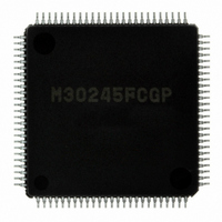
M30245FCGP#U1 Renesas Electronics America, M30245FCGP#U1 Datasheet - Page 200

M30245FCGP#U1
Manufacturer Part Number
M30245FCGP#U1
Description
IC M16C/24 MCU FLSH 128K 100LQFP
Manufacturer
Renesas Electronics America
Series
M16C™ M16C/20r
Datasheet
1.M30245FCGPU1.pdf
(268 pages)
Specifications of M30245FCGP#U1
Core Processor
M16C/60
Core Size
16-Bit
Speed
16MHz
Connectivity
I²C, SPI, SSI, UART/USART, USB
Peripherals
DMA, PWM, WDT
Number Of I /o
82
Program Memory Size
128KB (128K x 8)
Program Memory Type
FLASH
Ram Size
10K x 8
Voltage - Supply (vcc/vdd)
3 V ~ 3.6 V
Data Converters
A/D 8x10b
Oscillator Type
Internal
Operating Temperature
-20°C ~ 85°C
Package / Case
100-LQFP
Package
100LQFP
Family Name
R8C
Maximum Speed
16 MHz
Operating Supply Voltage
3.3 V
Data Bus Width
16 Bit
Number Of Programmable I/os
82
Interface Type
USB/UART/I2C/SPI
On-chip Adc
8-chx10-bit
Number Of Timers
5
Lead Free Status / RoHS Status
Lead free / RoHS Compliant
Eeprom Size
-
Available stocks
Company
Part Number
Manufacturer
Quantity
Price
- Current page: 200 of 268
- Download datasheet (3Mb)
M30245 Group
Figure 1.150. Flash memory control register
Figure 1.151. CPU rewrite mode set/reset flowchart
Rev.2.00
REJ03B0005-0200
Oct 16, 2006
Flash memory control register 0
b7
b6
page 198 of 264
b5
b4
0
Note 1: During CPU rewrite mode, set the main clock frequency to 6.25MHz or less using the main clock division
Note 2: For CPU rewrite mode select bit to be set to "1", the user needs to write a "0" and then a "1" to it in
Note 3: Before exiting the CPU rewrite mode after completing erase or program operation, always be sure to
Note 4: "1" can be set. However, when this bit is "1", user ROM area is accessed.
(Subsequent operations are executed by control
b3
Jump to transferred control program in RAM
Single-chip mode, memory expansion
Set processor mode register (Note 1)
b2
register (addresses 0006
succession. When it is not this procedure, it is not enacted in "1". This is necessary to ensure that no
interrupt or DMA transfer will be executed during the interval. Use the program except in the internal
flash memory for write to this bit. Also write to this bit when NMI pin is "H" level.
execute a read array command or reset the flash memory
Transfer CPU rewrite mode control
b1
program to internal RAM
program in this RAM)
mode, or boot mode
Program in ROM
b0
Note 1: To set this bit to "1", the user must write "0" and then "1" to it in succession. This bit is not
Note 2: To set this bit to "1", the user must write "0" and then "1" to it in succession when the CPU
Note 3: Effective only when CPU rewrite mode select bit "1". Set this bit to "1" and then "0" in
Note 4: Effective only in boot mode. Use a control program that is not in the internal flash memory
FMR00
FMR01
FMR02
FMR03
Reserved
FMR05
Nothing is assigned. Write "0" when writing to these bits.
The value is indeterminate if read.
Start
Bit Symbol
*1
Symbol
FMR0
set to "1" unless this sequence has been performed. This is necessary to ensure that no
interrupt or DMA transfer are executed during the interval. Use the control program except
in the internal flash memory for writing to this bit. Also, write to this bit when the NMI pin
is "H" level.
rewrite mode select bit = "1". This bit is not set to "1" unless this sequence has been
performed. This is necessary to ensure that no interrupt or DMA transfer are executed
during the interval.
succession.
when writing to this bit.
16
and 0007
RY/BY status bit
CPU rewrite mode select bit
(Note 1)
Lock bit disable bit
(Note 2)
Flash memory reset bit
(Note 3)
User ROM area select bit
(Note 4).
Bit Name
16
).
.
Execute read array command or reset flash
memory by setting flash memory reset bit (by
writing "1" and then "0" in succession) (Note 3)
Set CPU rewrite mode select bit to "1" (by
writing "0" and then "1" in succession)(Note 2)
(Boot mode only)
Write "0" to user ROM area select bit (Note 4)
Using software command execute erase,
program, or other operation
(Set lock bit disable bit as required)
Write "0" to CPU rewrite mode select bit
(Boot mode only)
Set user ROM area select bit to "1"
Address
02F7
0 : Busy (overwrite or erase)
1 : Ready
0 : Normal mode
(invalid software commands)
1 : CPU rewrite mode
(software command accepted)
0 : Enabled
1 : Disabled
0 : Normal operation
1 : Reset
Must always be "0"
0 : Boot ROM area accessed
1 : User ROM area accessed
16
Program in RAM
Function
End
*1
XX000001
When reset
R W
O O
O O
O O
O O
O O
O X
_ _
16
CPU Rewrite Mode
Related parts for M30245FCGP#U1
Image
Part Number
Description
Manufacturer
Datasheet
Request
R

Part Number:
Description:
KIT STARTER FOR M16C/29
Manufacturer:
Renesas Electronics America
Datasheet:

Part Number:
Description:
KIT STARTER FOR R8C/2D
Manufacturer:
Renesas Electronics America
Datasheet:

Part Number:
Description:
R0K33062P STARTER KIT
Manufacturer:
Renesas Electronics America
Datasheet:

Part Number:
Description:
KIT STARTER FOR R8C/23 E8A
Manufacturer:
Renesas Electronics America
Datasheet:

Part Number:
Description:
KIT STARTER FOR R8C/25
Manufacturer:
Renesas Electronics America
Datasheet:

Part Number:
Description:
KIT STARTER H8S2456 SHARPE DSPLY
Manufacturer:
Renesas Electronics America
Datasheet:

Part Number:
Description:
KIT STARTER FOR R8C38C
Manufacturer:
Renesas Electronics America
Datasheet:

Part Number:
Description:
KIT STARTER FOR R8C35C
Manufacturer:
Renesas Electronics America
Datasheet:

Part Number:
Description:
KIT STARTER FOR R8CL3AC+LCD APPS
Manufacturer:
Renesas Electronics America
Datasheet:

Part Number:
Description:
KIT STARTER FOR RX610
Manufacturer:
Renesas Electronics America
Datasheet:

Part Number:
Description:
KIT STARTER FOR R32C/118
Manufacturer:
Renesas Electronics America
Datasheet:

Part Number:
Description:
KIT DEV RSK-R8C/26-29
Manufacturer:
Renesas Electronics America
Datasheet:

Part Number:
Description:
KIT STARTER FOR SH7124
Manufacturer:
Renesas Electronics America
Datasheet:

Part Number:
Description:
KIT STARTER FOR H8SX/1622
Manufacturer:
Renesas Electronics America
Datasheet:


