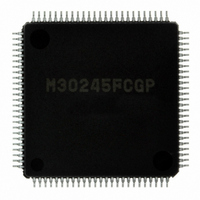
M30245FCGP#U1 Renesas Electronics America, M30245FCGP#U1 Datasheet - Page 40

M30245FCGP#U1
Manufacturer Part Number
M30245FCGP#U1
Description
IC M16C/24 MCU FLSH 128K 100LQFP
Manufacturer
Renesas Electronics America
Series
M16C™ M16C/20r
Datasheet
1.M30245FCGPU1.pdf
(268 pages)
Specifications of M30245FCGP#U1
Core Processor
M16C/60
Core Size
16-Bit
Speed
16MHz
Connectivity
I²C, SPI, SSI, UART/USART, USB
Peripherals
DMA, PWM, WDT
Number Of I /o
82
Program Memory Size
128KB (128K x 8)
Program Memory Type
FLASH
Ram Size
10K x 8
Voltage - Supply (vcc/vdd)
3 V ~ 3.6 V
Data Converters
A/D 8x10b
Oscillator Type
Internal
Operating Temperature
-20°C ~ 85°C
Package / Case
100-LQFP
Package
100LQFP
Family Name
R8C
Maximum Speed
16 MHz
Operating Supply Voltage
3.3 V
Data Bus Width
16 Bit
Number Of Programmable I/os
82
Interface Type
USB/UART/I2C/SPI
On-chip Adc
8-chx10-bit
Number Of Timers
5
Lead Free Status / RoHS Status
Lead free / RoHS Compliant
Eeprom Size
-
Available stocks
Company
Part Number
Manufacturer
Quantity
Price
- Current page: 40 of 268
- Download datasheet (3Mb)
M30245 Group
System Clock
Table 1.23. Main clock-generating circuits
Figure 1.18. Block diagram of the clock-generating circuit
Rev.2.00
REJ03B0005-0200
Note: Insert a damping resistor if required. The resistance will vary depending on the oscillator and the oscillation drive
(Built-in feedback resistor)
Clock-generating Circuit
X
The clock generating circuit contains two oscillator circuits that supply the operating clock sources to the CPU and
internal peripheral units. Figure 1.18 shows the block diagram of the clock-generating circuit. Table 1.23 lists the main
clock-generating circuits.
IN
When the oscillation drive capacity is set to low, check that oscillation is stable.
capacity setting. Use the value recommended by the maker of the oscillator.
Microcomputer
C
IN
Oct 16, 2006
reset
Software
RESET
Interrupt request
level judgment
output
NMI
X
page 38 of 264
OUT
WAIT instruction
(Note)
R
C
CM10 "1"
Write signal
d
OUT
CM0i :
CM1i :
FSCCRi: Bit i at address 03DB
Bit i at address 0006
Bit i at address 0007
CM05
S
R
S
R
Q
Q
CM04
16
16
16
X
IN
Main clock
FSCCR0=1
FSCCR0=0
Xcin
X
a
OUT
Sub clock
CM02
Synthesizer
Frequency
Circuit
CM06=0
CM17,CM16=00
1/2
Xcout
CM06=0
CM17,CM16=01
fsyn
1/2
CM06=0
CM17,CM16=10
1/32
a
1/2
Divider
b
fc32
fc
c
b
CM06=1
d
f
f
usb (48MHz)
AD
f
32
f
f
CM07=1
8
1/2
Vcc
Vss
1
fc
CM07=0
Details of divider
Externally derived clock
X
IN
CM06=0
CM17,CM16=11
f
f
f
1
8
32
SIO2
SIO2
1/2
Microcomputer
SIO2
BCLK
c
d
System Clock
Open
X
OUT
Related parts for M30245FCGP#U1
Image
Part Number
Description
Manufacturer
Datasheet
Request
R

Part Number:
Description:
KIT STARTER FOR M16C/29
Manufacturer:
Renesas Electronics America
Datasheet:

Part Number:
Description:
KIT STARTER FOR R8C/2D
Manufacturer:
Renesas Electronics America
Datasheet:

Part Number:
Description:
R0K33062P STARTER KIT
Manufacturer:
Renesas Electronics America
Datasheet:

Part Number:
Description:
KIT STARTER FOR R8C/23 E8A
Manufacturer:
Renesas Electronics America
Datasheet:

Part Number:
Description:
KIT STARTER FOR R8C/25
Manufacturer:
Renesas Electronics America
Datasheet:

Part Number:
Description:
KIT STARTER H8S2456 SHARPE DSPLY
Manufacturer:
Renesas Electronics America
Datasheet:

Part Number:
Description:
KIT STARTER FOR R8C38C
Manufacturer:
Renesas Electronics America
Datasheet:

Part Number:
Description:
KIT STARTER FOR R8C35C
Manufacturer:
Renesas Electronics America
Datasheet:

Part Number:
Description:
KIT STARTER FOR R8CL3AC+LCD APPS
Manufacturer:
Renesas Electronics America
Datasheet:

Part Number:
Description:
KIT STARTER FOR RX610
Manufacturer:
Renesas Electronics America
Datasheet:

Part Number:
Description:
KIT STARTER FOR R32C/118
Manufacturer:
Renesas Electronics America
Datasheet:

Part Number:
Description:
KIT DEV RSK-R8C/26-29
Manufacturer:
Renesas Electronics America
Datasheet:

Part Number:
Description:
KIT STARTER FOR SH7124
Manufacturer:
Renesas Electronics America
Datasheet:

Part Number:
Description:
KIT STARTER FOR H8SX/1622
Manufacturer:
Renesas Electronics America
Datasheet:


