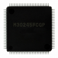
M30245FCGP#U1 Renesas Electronics America, M30245FCGP#U1 Datasheet - Page 193

M30245FCGP#U1
Manufacturer Part Number
M30245FCGP#U1
Description
IC M16C/24 MCU FLSH 128K 100LQFP
Manufacturer
Renesas Electronics America
Series
M16C™ M16C/20r
Datasheet
1.M30245FCGPU1.pdf
(268 pages)
Specifications of M30245FCGP#U1
Core Processor
M16C/60
Core Size
16-Bit
Speed
16MHz
Connectivity
I²C, SPI, SSI, UART/USART, USB
Peripherals
DMA, PWM, WDT
Number Of I /o
82
Program Memory Size
128KB (128K x 8)
Program Memory Type
FLASH
Ram Size
10K x 8
Voltage - Supply (vcc/vdd)
3 V ~ 3.6 V
Data Converters
A/D 8x10b
Oscillator Type
Internal
Operating Temperature
-20°C ~ 85°C
Package / Case
100-LQFP
Package
100LQFP
Family Name
R8C
Maximum Speed
16 MHz
Operating Supply Voltage
3.3 V
Data Bus Width
16 Bit
Number Of Programmable I/os
82
Interface Type
USB/UART/I2C/SPI
On-chip Adc
8-chx10-bit
Number Of Timers
5
Lead Free Status / RoHS Status
Lead free / RoHS Compliant
Eeprom Size
-
Available stocks
Company
Part Number
Manufacturer
Quantity
Price
- Current page: 193 of 268
- Download datasheet (3Mb)
M30245 Group
Figure 1.144. Example connections to AND flash memory
Table 1.66. AND flash function table
Rev.2.00
REJ03B0005-0200
WECTL, OECTL
Sample AND Flash Control Algorithms
Figure 1.144 shows an example of how to connect an AND type flash memory to the M30245 AND Flash Conntrol circuit.
Figures 1.145 and 1.146 show flow charts describing sample read and write (program) operations of AND flash
memory. Please consult the M5M29F5611VP AND flash memory product specification for a detailed description of
it’s design and control.
00
01
10
11
Oct 16, 2006
"L" pulse during AND_DATA read cycle
"L" pulse during AND_DATA read cycle
page 191 of 264
AND_OE
"L"
P0 (AND_DATA)
P1
P1
P1
M30245
1
P1
P1
P1
P1
2
0
(AND_WE)
(AND_SC)
(AND_OE)
3
4
7
6
(GP I/O)
(GP I/O)
(GP I/O)
(GP I/O)
"L" pulse during AND_DATA write cycle
"L" pulse during AND_DATA write cycle
AND_WE
Inhibited
"H"
HN29V2561 1 A
HN29V5121 1 A
DQ(0:7)
SC
WE
OE
CE
CDE
R/B
RES
"H" pulse during AND_DATA write cycle
"H" pulse during AND_DATA read cycle
And Flash Control Circuit
AND_SC
"L"
Related parts for M30245FCGP#U1
Image
Part Number
Description
Manufacturer
Datasheet
Request
R

Part Number:
Description:
KIT STARTER FOR M16C/29
Manufacturer:
Renesas Electronics America
Datasheet:

Part Number:
Description:
KIT STARTER FOR R8C/2D
Manufacturer:
Renesas Electronics America
Datasheet:

Part Number:
Description:
R0K33062P STARTER KIT
Manufacturer:
Renesas Electronics America
Datasheet:

Part Number:
Description:
KIT STARTER FOR R8C/23 E8A
Manufacturer:
Renesas Electronics America
Datasheet:

Part Number:
Description:
KIT STARTER FOR R8C/25
Manufacturer:
Renesas Electronics America
Datasheet:

Part Number:
Description:
KIT STARTER H8S2456 SHARPE DSPLY
Manufacturer:
Renesas Electronics America
Datasheet:

Part Number:
Description:
KIT STARTER FOR R8C38C
Manufacturer:
Renesas Electronics America
Datasheet:

Part Number:
Description:
KIT STARTER FOR R8C35C
Manufacturer:
Renesas Electronics America
Datasheet:

Part Number:
Description:
KIT STARTER FOR R8CL3AC+LCD APPS
Manufacturer:
Renesas Electronics America
Datasheet:

Part Number:
Description:
KIT STARTER FOR RX610
Manufacturer:
Renesas Electronics America
Datasheet:

Part Number:
Description:
KIT STARTER FOR R32C/118
Manufacturer:
Renesas Electronics America
Datasheet:

Part Number:
Description:
KIT DEV RSK-R8C/26-29
Manufacturer:
Renesas Electronics America
Datasheet:

Part Number:
Description:
KIT STARTER FOR SH7124
Manufacturer:
Renesas Electronics America
Datasheet:

Part Number:
Description:
KIT STARTER FOR H8SX/1622
Manufacturer:
Renesas Electronics America
Datasheet:


