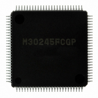
M30245FCGP#U1 Renesas Electronics America, M30245FCGP#U1 Datasheet - Page 176

M30245FCGP#U1
Manufacturer Part Number
M30245FCGP#U1
Description
IC M16C/24 MCU FLSH 128K 100LQFP
Manufacturer
Renesas Electronics America
Series
M16C™ M16C/20r
Datasheet
1.M30245FCGPU1.pdf
(268 pages)
Specifications of M30245FCGP#U1
Core Processor
M16C/60
Core Size
16-Bit
Speed
16MHz
Connectivity
I²C, SPI, SSI, UART/USART, USB
Peripherals
DMA, PWM, WDT
Number Of I /o
82
Program Memory Size
128KB (128K x 8)
Program Memory Type
FLASH
Ram Size
10K x 8
Voltage - Supply (vcc/vdd)
3 V ~ 3.6 V
Data Converters
A/D 8x10b
Oscillator Type
Internal
Operating Temperature
-20°C ~ 85°C
Package / Case
100-LQFP
Package
100LQFP
Family Name
R8C
Maximum Speed
16 MHz
Operating Supply Voltage
3.3 V
Data Bus Width
16 Bit
Number Of Programmable I/os
82
Interface Type
USB/UART/I2C/SPI
On-chip Adc
8-chx10-bit
Number Of Timers
5
Lead Free Status / RoHS Status
Lead free / RoHS Compliant
Eeprom Size
-
Available stocks
Company
Part Number
Manufacturer
Quantity
Price
- Current page: 176 of 268
- Download datasheet (3Mb)
M30245 Group
Table 1.61. Repeat sweep mode 1 specifications
Rev.2.00
REJ03B0005-0200
Function
Start condition
Stop condition
Interrupt request
generation timing
Input pin
Pin emphasis
A/D converter results
Repeat sweep mode 1
Resolution select function
Sample and hold
Power consumption reduction function
Precautions
In repeat sweep mode 1, all pins are used for A/D conversion with emphasis on the pin or pins selected using the A/
D sweep pin select bit. Table 1.61 shows the specifications of repeat sweep mode 1.
8 or 10-bit mode select bit of AD control register 1 (bit 3 at address 03D7
When set to 10-bit precision, the low 8-bits are stored in the even addresses and the high 2 bits in the odd ad-
dresses. When set to 8-bit precision, the low 8 bits are stored in the even addresses.
Sample and hold is selected by setting bit 0 of the AD control register 2 (address 03D4
hold is selected, the rate of conversion of each pin increases. As a result, a 28 f
resolution and 33 f
be sure to specify before starting A/D conversion whether sample and hold is to be used.
The V
from the reference voltage pin (V
resistance ladder from V
only after connecting V
•
when A/D conversion is stopped (before a trigger occurs). When the V
wait 1 µs or longer before starting A/D conversion.
•
Write to each bit (except bit 6) of AD control register 0, AD control register 1, and to bit 0 of AD control register 2
When changing A/D operation mode, select the analog input pin again.
Oct 16, 2006
Item
REF
connect bit (bit 5 at addresses 03D7
AD
page 174 of 264
with 10-bit resolution. Sample and hold can be selected in all modes. However, in all modes,
REF
All pinsperform repeat sweep A/D conversion with emphasis on the pin or pins selected by
the A/D sweep pin select bit.
Example: AN
Writing "1" to A/D conversion start flag.
Writing "0" to A/D conversion start flag.
None generated.
AN
AN
Read AD register corresponding to selected pin (at any time).
REF
. Do not write A/D conversion start flag and V
0
0
, reducing the power dissipation. When using the A/D converter, start A/D conversion
to AN
(1 pin) AN
REF
7
.
) when the A/D converter is not used. This stops any current from flowing into the
0
selected:
0
and AN
16
1
) can be used to isolate the resistance ladder of the A/D converter
(2 pins), AN
AN
0
AN
0
Specification
to AN
1
2
(3 pins), AN
REF
AN
REF
16
0
connection bit is changed from "0" to "1",
)
connect bit to "1" at the same time.
AD
AN
0
cycle is achieved with 8-bit
to AN
2
16
3
) to "1". When sample and
(4 pins).
AN
0
A/D converter
AN
3
etc.
Related parts for M30245FCGP#U1
Image
Part Number
Description
Manufacturer
Datasheet
Request
R

Part Number:
Description:
KIT STARTER FOR M16C/29
Manufacturer:
Renesas Electronics America
Datasheet:

Part Number:
Description:
KIT STARTER FOR R8C/2D
Manufacturer:
Renesas Electronics America
Datasheet:

Part Number:
Description:
R0K33062P STARTER KIT
Manufacturer:
Renesas Electronics America
Datasheet:

Part Number:
Description:
KIT STARTER FOR R8C/23 E8A
Manufacturer:
Renesas Electronics America
Datasheet:

Part Number:
Description:
KIT STARTER FOR R8C/25
Manufacturer:
Renesas Electronics America
Datasheet:

Part Number:
Description:
KIT STARTER H8S2456 SHARPE DSPLY
Manufacturer:
Renesas Electronics America
Datasheet:

Part Number:
Description:
KIT STARTER FOR R8C38C
Manufacturer:
Renesas Electronics America
Datasheet:

Part Number:
Description:
KIT STARTER FOR R8C35C
Manufacturer:
Renesas Electronics America
Datasheet:

Part Number:
Description:
KIT STARTER FOR R8CL3AC+LCD APPS
Manufacturer:
Renesas Electronics America
Datasheet:

Part Number:
Description:
KIT STARTER FOR RX610
Manufacturer:
Renesas Electronics America
Datasheet:

Part Number:
Description:
KIT STARTER FOR R32C/118
Manufacturer:
Renesas Electronics America
Datasheet:

Part Number:
Description:
KIT DEV RSK-R8C/26-29
Manufacturer:
Renesas Electronics America
Datasheet:

Part Number:
Description:
KIT STARTER FOR SH7124
Manufacturer:
Renesas Electronics America
Datasheet:

Part Number:
Description:
KIT STARTER FOR H8SX/1622
Manufacturer:
Renesas Electronics America
Datasheet:


