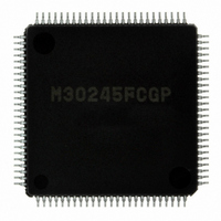
M30245FCGP#U1 Renesas Electronics America, M30245FCGP#U1 Datasheet - Page 160

M30245FCGP#U1
Manufacturer Part Number
M30245FCGP#U1
Description
IC M16C/24 MCU FLSH 128K 100LQFP
Manufacturer
Renesas Electronics America
Series
M16C™ M16C/20r
Datasheet
1.M30245FCGPU1.pdf
(268 pages)
Specifications of M30245FCGP#U1
Core Processor
M16C/60
Core Size
16-Bit
Speed
16MHz
Connectivity
I²C, SPI, SSI, UART/USART, USB
Peripherals
DMA, PWM, WDT
Number Of I /o
82
Program Memory Size
128KB (128K x 8)
Program Memory Type
FLASH
Ram Size
10K x 8
Voltage - Supply (vcc/vdd)
3 V ~ 3.6 V
Data Converters
A/D 8x10b
Oscillator Type
Internal
Operating Temperature
-20°C ~ 85°C
Package / Case
100-LQFP
Package
100LQFP
Family Name
R8C
Maximum Speed
16 MHz
Operating Supply Voltage
3.3 V
Data Bus Width
16 Bit
Number Of Programmable I/os
82
Interface Type
USB/UART/I2C/SPI
On-chip Adc
8-chx10-bit
Number Of Timers
5
Lead Free Status / RoHS Status
Lead free / RoHS Compliant
Eeprom Size
-
Available stocks
Company
Part Number
Manufacturer
Quantity
Price
- Current page: 160 of 268
- Download datasheet (3Mb)
M30245 Group
Figure 1.117. Transmit and receive data (and WS) synchronized to SCK
Rev.2.00
REJ03B0005-0200
The following features are supported via firmware controlled mode bits:
• Simultaneous transmit and receive (through separate transmit and receive pins) synchronized to the same SCK
and WS signals.
• Transmit/receive data and WS synchronized to the rising edge or the falling edge of SCK as shown in Figure 1.117.
• Transmit and receive synchronized to the rising or the falling edge of WS as shown in Figure 1.118.
• Normal or delayed WS: WS transitions one SCK period before a channel change (normal mode) or concurrently
with a channel change (delayed mode) as shown in Figure 1.119.
• Automatic interrupt on a channel change and on every access to the data buffer (transmit/receive) until each data
buffer byte is accessed.
• Channel widths of 32, 24, and 16 bits.
• MSB or LSB first transmit and receive.
• Multiple receive formats: if the number of SCKs in a WS high/low period is less than the channel width, the data can
be placed either MSB or LSB justified as shown in Figure 1.120.
• Rate feedback: when used with the USB interface, the Serial Sound Interface can count the number of WS’s or
SCK’s per USB frame.
Data/WS synchronized to rising edge (SCKP = 1)
Data
WS
Data/WS synchronized to falling edge (SCKP = 0)
Data
SCK
SCK
WS
Oct 16, 2006
page 158 of 264
Serial Sound Interface
Related parts for M30245FCGP#U1
Image
Part Number
Description
Manufacturer
Datasheet
Request
R

Part Number:
Description:
KIT STARTER FOR M16C/29
Manufacturer:
Renesas Electronics America
Datasheet:

Part Number:
Description:
KIT STARTER FOR R8C/2D
Manufacturer:
Renesas Electronics America
Datasheet:

Part Number:
Description:
R0K33062P STARTER KIT
Manufacturer:
Renesas Electronics America
Datasheet:

Part Number:
Description:
KIT STARTER FOR R8C/23 E8A
Manufacturer:
Renesas Electronics America
Datasheet:

Part Number:
Description:
KIT STARTER FOR R8C/25
Manufacturer:
Renesas Electronics America
Datasheet:

Part Number:
Description:
KIT STARTER H8S2456 SHARPE DSPLY
Manufacturer:
Renesas Electronics America
Datasheet:

Part Number:
Description:
KIT STARTER FOR R8C38C
Manufacturer:
Renesas Electronics America
Datasheet:

Part Number:
Description:
KIT STARTER FOR R8C35C
Manufacturer:
Renesas Electronics America
Datasheet:

Part Number:
Description:
KIT STARTER FOR R8CL3AC+LCD APPS
Manufacturer:
Renesas Electronics America
Datasheet:

Part Number:
Description:
KIT STARTER FOR RX610
Manufacturer:
Renesas Electronics America
Datasheet:

Part Number:
Description:
KIT STARTER FOR R32C/118
Manufacturer:
Renesas Electronics America
Datasheet:

Part Number:
Description:
KIT DEV RSK-R8C/26-29
Manufacturer:
Renesas Electronics America
Datasheet:

Part Number:
Description:
KIT STARTER FOR SH7124
Manufacturer:
Renesas Electronics America
Datasheet:

Part Number:
Description:
KIT STARTER FOR H8SX/1622
Manufacturer:
Renesas Electronics America
Datasheet:


