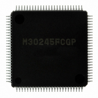
M30245FCGP#U1 Renesas Electronics America, M30245FCGP#U1 Datasheet - Page 74

M30245FCGP#U1
Manufacturer Part Number
M30245FCGP#U1
Description
IC M16C/24 MCU FLSH 128K 100LQFP
Manufacturer
Renesas Electronics America
Series
M16C™ M16C/20r
Datasheet
1.M30245FCGPU1.pdf
(268 pages)
Specifications of M30245FCGP#U1
Core Processor
M16C/60
Core Size
16-Bit
Speed
16MHz
Connectivity
I²C, SPI, SSI, UART/USART, USB
Peripherals
DMA, PWM, WDT
Number Of I /o
82
Program Memory Size
128KB (128K x 8)
Program Memory Type
FLASH
Ram Size
10K x 8
Voltage - Supply (vcc/vdd)
3 V ~ 3.6 V
Data Converters
A/D 8x10b
Oscillator Type
Internal
Operating Temperature
-20°C ~ 85°C
Package / Case
100-LQFP
Package
100LQFP
Family Name
R8C
Maximum Speed
16 MHz
Operating Supply Voltage
3.3 V
Data Bus Width
16 Bit
Number Of Programmable I/os
82
Interface Type
USB/UART/I2C/SPI
On-chip Adc
8-chx10-bit
Number Of Timers
5
Lead Free Status / RoHS Status
Lead free / RoHS Compliant
Eeprom Size
-
Available stocks
Company
Part Number
Manufacturer
Quantity
Price
- Current page: 74 of 268
- Download datasheet (3Mb)
M30245 Group
Rev.2.00
REJ03B0005-0200
USB Endpoint FIFOs
USB Suspend Interrupt
EP0 FIFO Operation
EP0 IN FIFO with control read continuous transfer mode disabled
The CPU writes "1" to the SET_IN_BUF_RDY bit of the EP0 CSR after the CPU finishes writing a data packet to the FIFO,
this updates the IN_BUF_RDY flag to "1". The USB FCU updates the IN_BUF_RDY flag to "0" after the packet has been
successfully transmitted to the host.
EP0 IN FIFO with control read continuous transfer mode enabled
The CPU writes "1" to the SET_IN_BUF_RDY bit of the EP0 CSR after the CPU finishes writing a data set (up to 128 bytes)
to the FIFO. This updates the IN_BUF_RDY flag to "1". The USB FCU sends out data packets equal to the EP0 MAXP size
one at a time, except for the last packet if the data set in the FIFO is not a multiple of EP0 MAXP. In this case the USB FCU
sends a short packet. The USB FCU updates the IN_BUF_RDY flag to "0" after the data set has been successfully transmitted
to the host.
The CPU reads data from EP0 OUT FIFO Data Register. The read pointer automatically increments by 2 in word
accessing mode or by 1 in byte accessing mode after a read. The CPU must only read data from the EP0 OUT FIFO
when the OUT_BUF_RDY flag of the EP0_CSR is "1".
When a SETUP packet is received, an EP0 interrupt is generated (both OUT_BUF_RDY and SETUP flags are set)
regardless of the continuous transfer mode bit setting.
EP0 OUT FIFO with control write continuous transfer mode disabled
The USB FCU updates the OUT_BUF_RDY flag to "1" after it has successfully received a data packet from the host. The
CPU writes "1" to CLR_OUT_BUF_RDY after the data packet has been unloaded from the FIFO by the CPU (updates the
OUT_BUF_RDY flag to a "0").
A USB Suspend Interrupt is generated when the USB FCU does not detect any bus activity on D+/D- (in J-state) for at
least 3ms.
The USB Suspend Interrupt Control register (SUSPIC) contains the USB Suspend Interrupt request bit and interrupt
priority select bits that are used to enable the interrupt and set its software priority level.
The USB FCU has a built-in 3.25 K bytes FIFO as an endpoint buffer. The EP0 (control endpoint) FIFO occupies
a fixed location (from 3K - 3.25K) with fixed buffer sizes (128 bytes each) for its IN and OUT data transfers. The other
8 endpoints (EP1 to EP4 IN and OUT) share a 3K bytes buffer. Each endpoint’s FIFO size and starting location (64
bytes) are programmable by the user. The sum of the 8 endpoint FIFOs can not exceed 3K bytes (3072 bytes).
Note: Throughout the USB Block specification, "data packet" is generally used when continuous mode is disabled;
"data set" (one or more data packets) is generally used when continuous mode is enabled. If a description applies
for both noncontinuous mode and continuous mode, "data set" is used.
Throughout the whole USB Block Specification, "FIFO" and "Buffer" are generally interchangeable terms.
The CPU writes data to the EP0 IN FIFO Data Register. The write pointer automatically increments by 2 in word
accessing mode or by 1 in byte accessing mode after a write. The CPU must only write data to the EP0 IN FIFO Data
Register and "1" to the SET_IN_BUF_RDY bit of the EP0 CSR when the IN_BUF_RDY flag is a "0". When a NULL packet
is required to complete a control read request, the CPU must write "1" to the SET_IN_BUF_RDY bit of EP0_CSR
without writing data to the EP0 IN FIFO Data Register.
Continuous transfer modes are available for EP0 Control Transfers.
Oct 16, 2006
page 72 of 264
Universal Serial Bus
Related parts for M30245FCGP#U1
Image
Part Number
Description
Manufacturer
Datasheet
Request
R

Part Number:
Description:
KIT STARTER FOR M16C/29
Manufacturer:
Renesas Electronics America
Datasheet:

Part Number:
Description:
KIT STARTER FOR R8C/2D
Manufacturer:
Renesas Electronics America
Datasheet:

Part Number:
Description:
R0K33062P STARTER KIT
Manufacturer:
Renesas Electronics America
Datasheet:

Part Number:
Description:
KIT STARTER FOR R8C/23 E8A
Manufacturer:
Renesas Electronics America
Datasheet:

Part Number:
Description:
KIT STARTER FOR R8C/25
Manufacturer:
Renesas Electronics America
Datasheet:

Part Number:
Description:
KIT STARTER H8S2456 SHARPE DSPLY
Manufacturer:
Renesas Electronics America
Datasheet:

Part Number:
Description:
KIT STARTER FOR R8C38C
Manufacturer:
Renesas Electronics America
Datasheet:

Part Number:
Description:
KIT STARTER FOR R8C35C
Manufacturer:
Renesas Electronics America
Datasheet:

Part Number:
Description:
KIT STARTER FOR R8CL3AC+LCD APPS
Manufacturer:
Renesas Electronics America
Datasheet:

Part Number:
Description:
KIT STARTER FOR RX610
Manufacturer:
Renesas Electronics America
Datasheet:

Part Number:
Description:
KIT STARTER FOR R32C/118
Manufacturer:
Renesas Electronics America
Datasheet:

Part Number:
Description:
KIT DEV RSK-R8C/26-29
Manufacturer:
Renesas Electronics America
Datasheet:

Part Number:
Description:
KIT STARTER FOR SH7124
Manufacturer:
Renesas Electronics America
Datasheet:

Part Number:
Description:
KIT STARTER FOR H8SX/1622
Manufacturer:
Renesas Electronics America
Datasheet:


