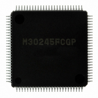
M30245FCGP#U1 Renesas Electronics America, M30245FCGP#U1 Datasheet - Page 256

M30245FCGP#U1
Manufacturer Part Number
M30245FCGP#U1
Description
IC M16C/24 MCU FLSH 128K 100LQFP
Manufacturer
Renesas Electronics America
Series
M16C™ M16C/20r
Datasheet
1.M30245FCGPU1.pdf
(268 pages)
Specifications of M30245FCGP#U1
Core Processor
M16C/60
Core Size
16-Bit
Speed
16MHz
Connectivity
I²C, SPI, SSI, UART/USART, USB
Peripherals
DMA, PWM, WDT
Number Of I /o
82
Program Memory Size
128KB (128K x 8)
Program Memory Type
FLASH
Ram Size
10K x 8
Voltage - Supply (vcc/vdd)
3 V ~ 3.6 V
Data Converters
A/D 8x10b
Oscillator Type
Internal
Operating Temperature
-20°C ~ 85°C
Package / Case
100-LQFP
Package
100LQFP
Family Name
R8C
Maximum Speed
16 MHz
Operating Supply Voltage
3.3 V
Data Bus Width
16 Bit
Number Of Programmable I/os
82
Interface Type
USB/UART/I2C/SPI
On-chip Adc
8-chx10-bit
Number Of Timers
5
Lead Free Status / RoHS Status
Lead free / RoHS Compliant
Eeprom Size
-
Available stocks
Company
Part Number
Manufacturer
Quantity
Price
- Current page: 256 of 268
- Download datasheet (3Mb)
M30245 Group
Rev.2.00
REJ03B0005-0200
Stop Mode and Wait Mode
Interrupts
Reading address 00000
Setting the stack pointer
The NMI interrupt
External interrupt
(1) When returning from stop mode by hardware reset, RESET pin must be set to “L” level until main clock oscillation is
(2) When switching to either wait mode or stop mode, instructions occupying four bytes either from the WAIT instruction
(3) When using low-speed mode and low power dissipation mode, set the WAIT peripheral function clock stop bit
(4) When using f
When maskable interrupt occurs, the CPU reads the interrupt information (the interrupt number and interrupt request
evel) in the interrupt sequence. The interrupt request bit of the interrupt written in address 00000
“0”.
Do not read address 00000
interrupt source request bit to “0”. Though the interrupt is generated, the interrupt routine may not be executed.
The value of the stack pointer immediately after reset is initialized to 0000
value in the stack pointer may cause program runaway. Be sure to set a value in the stack pointer before accepting
an interrupt.
When using the NMI interrupt, initialize the stack pointer at the beginning of a program. Generating any interrupts
including the NMI interrupt is prohibited for the first instruction immediately after reset.
The NMI interrupt can not be disabled. Be sure to connect NMI pin to Vcc with a pull-up resistor if unused. Do not go
into stop mode when the NMI pin set to “L”.
The NMI pin also serves as P8
value to be read. Reading this pin is only to be used for establishing the pin level when the NMI interrupt is input.
Do not reset the CPU with the input to the NMI pin in the “L” state.
Do not attempt to go into stop mode when the input to the NMI pin is in “L” state. When the input to the NMI is in “L”
state, CM10 is fixed to “0” thereby refusing to go into stop mode.
Do not attempt to go into wait mode when the input to the NMI pin is in “L” state. When the input to the NMI pin is in
“L” state, the CPU stops but the oscillation does not. This action does not save power. When this occurs, the CPU is
returned to the normal state by a later interrupt.
Signals input to the NMI pin require an “L” level of (2 clocks + 300nS) or more from the operation clock of the CPU.
Either an “H” or “L” level of at least 250 ns width is necessary for the signal input to pins INT0 to INT2 regardless of
the CPU operation clock.
When the polarity of the INT0 to INT2 pins is changed, the interrupt request bit is sometimes set to “1”. After chang-
ing the polarity, reset the interrupt request bit to “0”. Figure 1.208 shows the procedure for changing the INT interrupt
generate factor.
stabilized.
or from the instruction that sets the all clock stop control bit to “1” within the instruction queue are prefetched and then
the program stops. So put at least four NOPs in succession either to the WAIT instruction or to the instruction that
sets the all clock stop control bit to “1”.
(CM02) to “1” and do not shift to wait mode.
frequency synthesizer control register to “0”).
_______
_______
_______
Oct 16, 2006
_______
_______
SYN
_______
page 254 of 264
as the internal system clock, change to f(X
16
________
_______
16
by software. Reading address 00000
5
, which is exclusively an input. Reading the contents of the P8 register allows the pin
________
_______
___________
_______
_______
_______
IN
16
) before entering to stop mode (set bit 0 of the
by software sets enabled highest priority
16
. Accepting an interrupt before setting a
________
_______
________
16
will then be set to
Usage Notes
_______
_______
Related parts for M30245FCGP#U1
Image
Part Number
Description
Manufacturer
Datasheet
Request
R

Part Number:
Description:
KIT STARTER FOR M16C/29
Manufacturer:
Renesas Electronics America
Datasheet:

Part Number:
Description:
KIT STARTER FOR R8C/2D
Manufacturer:
Renesas Electronics America
Datasheet:

Part Number:
Description:
R0K33062P STARTER KIT
Manufacturer:
Renesas Electronics America
Datasheet:

Part Number:
Description:
KIT STARTER FOR R8C/23 E8A
Manufacturer:
Renesas Electronics America
Datasheet:

Part Number:
Description:
KIT STARTER FOR R8C/25
Manufacturer:
Renesas Electronics America
Datasheet:

Part Number:
Description:
KIT STARTER H8S2456 SHARPE DSPLY
Manufacturer:
Renesas Electronics America
Datasheet:

Part Number:
Description:
KIT STARTER FOR R8C38C
Manufacturer:
Renesas Electronics America
Datasheet:

Part Number:
Description:
KIT STARTER FOR R8C35C
Manufacturer:
Renesas Electronics America
Datasheet:

Part Number:
Description:
KIT STARTER FOR R8CL3AC+LCD APPS
Manufacturer:
Renesas Electronics America
Datasheet:

Part Number:
Description:
KIT STARTER FOR RX610
Manufacturer:
Renesas Electronics America
Datasheet:

Part Number:
Description:
KIT STARTER FOR R32C/118
Manufacturer:
Renesas Electronics America
Datasheet:

Part Number:
Description:
KIT DEV RSK-R8C/26-29
Manufacturer:
Renesas Electronics America
Datasheet:

Part Number:
Description:
KIT STARTER FOR SH7124
Manufacturer:
Renesas Electronics America
Datasheet:

Part Number:
Description:
KIT STARTER FOR H8SX/1622
Manufacturer:
Renesas Electronics America
Datasheet:


