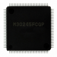
M30245FCGP#U1 Renesas Electronics America, M30245FCGP#U1 Datasheet - Page 151

M30245FCGP#U1
Manufacturer Part Number
M30245FCGP#U1
Description
IC M16C/24 MCU FLSH 128K 100LQFP
Manufacturer
Renesas Electronics America
Series
M16C™ M16C/20r
Datasheet
1.M30245FCGPU1.pdf
(268 pages)
Specifications of M30245FCGP#U1
Core Processor
M16C/60
Core Size
16-Bit
Speed
16MHz
Connectivity
I²C, SPI, SSI, UART/USART, USB
Peripherals
DMA, PWM, WDT
Number Of I /o
82
Program Memory Size
128KB (128K x 8)
Program Memory Type
FLASH
Ram Size
10K x 8
Voltage - Supply (vcc/vdd)
3 V ~ 3.6 V
Data Converters
A/D 8x10b
Oscillator Type
Internal
Operating Temperature
-20°C ~ 85°C
Package / Case
100-LQFP
Package
100LQFP
Family Name
R8C
Maximum Speed
16 MHz
Operating Supply Voltage
3.3 V
Data Bus Width
16 Bit
Number Of Programmable I/os
82
Interface Type
USB/UART/I2C/SPI
On-chip Adc
8-chx10-bit
Number Of Timers
5
Lead Free Status / RoHS Status
Lead free / RoHS Compliant
Eeprom Size
-
Available stocks
Company
Part Number
Manufacturer
Quantity
Price
- Current page: 151 of 268
- Download datasheet (3Mb)
M30245 Group
Table 1.51. Functions changed by clock phase set bits
Figure 1.108. Function changed by clock phase set bits
Rev.2.00
REJ03B0005-0200
SCL initial and last value
Transfer interrupt factor
Data transfer times from UART
receive shift register to receive buffer
register
UARTi Special Mode Register 3 (UiSMR3)
When UART transmit/receive is started using this function, the content of the transmit buffer available flag does not
change. Also, to use this function, select an external clock as the transfer clock. This bit is unavailable when SCLi is
external clock.
Bit 5 is SCL wait output bit 2. When this bit is set to "1" and serial I/O is selected, an "L" level can be output from the SCLi
pin even during UART operation. When this bit is set to "0", the "L" output from the SCLi pin is cancelled and the UARTi
clock is input and output. This bit is unavailable when SCLi is external clock.
Bit 6 is the SDA output disable bit. When this bit is set to "1", the SDAi pin is forced to high impedance. Overwrite this bit
at the rise of the UART transfer clock. The arbitration lost detection flag may be set.
Bit 0 : Not used in I
Bit 1 is the clock phase set bit. When both the I
of UiSMR2) are "1", functions changed by these bits are shown in Table 1.51 and Figure 1.108.
Bit 2 : Not used in I
Bit 3 : Not used in I
Bit 4 : Not used in I
Bit 5 to 7 are the I
set the f(Xin) delay to 2 to 8 cycles.
Oct 16, 2006
Function
2
C SDAi digital delay setting bits. By setting these bits, it is possible to turn the SDAi delay OFF or
2
2
2
2
• CKPH= "0" (IICM=1, IICM2=1)
• CKPH= "1" (IICM=1, IICM2=1)
C bus interface mode. See "SPI mode" section.
C bus interface mode.
C bus interface mode. See "SPI mode" section.
C bus interface mode. See "SPI mode" section
SCL
SDA
SCL
SDA
page 149 of 264
(Internal clock, transfer data 9 bits long and MSB first selected.)
(Internal clock, transfer data 9 bits long and MSB first selected.)
D
D
7
7
Initial value = "H", last value = "H"
Rising edge of 9th bit
Falling edge of 9th bit
D
D
6
6
CKPH=0, IICM=1, IICM2=1
D
D
5
5
2
C mode select bit (bit 0 of UiSMR) and the I
D
D
4
4
D
D
3
3
D
D
2
2
Transfer to UiRB register
Receive interrupt
Receive interrupt
D
D
1
1
Transfer to UiRB register
D
D
0
0
D
D
Initial value = "L", last value = "L"
Falling edge of 10th bit
Two-times: falling edge of 9th bit and
rising edge of 9th bit
Transmit interrupt
8
8
Transmit interrupt
CKPH=1, IICM=1, IICM2=1
I
2
C Bus interface mode
2
C mode select bit 2 (bit 0
Related parts for M30245FCGP#U1
Image
Part Number
Description
Manufacturer
Datasheet
Request
R

Part Number:
Description:
KIT STARTER FOR M16C/29
Manufacturer:
Renesas Electronics America
Datasheet:

Part Number:
Description:
KIT STARTER FOR R8C/2D
Manufacturer:
Renesas Electronics America
Datasheet:

Part Number:
Description:
R0K33062P STARTER KIT
Manufacturer:
Renesas Electronics America
Datasheet:

Part Number:
Description:
KIT STARTER FOR R8C/23 E8A
Manufacturer:
Renesas Electronics America
Datasheet:

Part Number:
Description:
KIT STARTER FOR R8C/25
Manufacturer:
Renesas Electronics America
Datasheet:

Part Number:
Description:
KIT STARTER H8S2456 SHARPE DSPLY
Manufacturer:
Renesas Electronics America
Datasheet:

Part Number:
Description:
KIT STARTER FOR R8C38C
Manufacturer:
Renesas Electronics America
Datasheet:

Part Number:
Description:
KIT STARTER FOR R8C35C
Manufacturer:
Renesas Electronics America
Datasheet:

Part Number:
Description:
KIT STARTER FOR R8CL3AC+LCD APPS
Manufacturer:
Renesas Electronics America
Datasheet:

Part Number:
Description:
KIT STARTER FOR RX610
Manufacturer:
Renesas Electronics America
Datasheet:

Part Number:
Description:
KIT STARTER FOR R32C/118
Manufacturer:
Renesas Electronics America
Datasheet:

Part Number:
Description:
KIT DEV RSK-R8C/26-29
Manufacturer:
Renesas Electronics America
Datasheet:

Part Number:
Description:
KIT STARTER FOR SH7124
Manufacturer:
Renesas Electronics America
Datasheet:

Part Number:
Description:
KIT STARTER FOR H8SX/1622
Manufacturer:
Renesas Electronics America
Datasheet:


