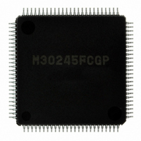
M30245FCGP#U1 Renesas Electronics America, M30245FCGP#U1 Datasheet - Page 214

M30245FCGP#U1
Manufacturer Part Number
M30245FCGP#U1
Description
IC M16C/24 MCU FLSH 128K 100LQFP
Manufacturer
Renesas Electronics America
Series
M16C™ M16C/20r
Datasheet
1.M30245FCGPU1.pdf
(268 pages)
Specifications of M30245FCGP#U1
Core Processor
M16C/60
Core Size
16-Bit
Speed
16MHz
Connectivity
I²C, SPI, SSI, UART/USART, USB
Peripherals
DMA, PWM, WDT
Number Of I /o
82
Program Memory Size
128KB (128K x 8)
Program Memory Type
FLASH
Ram Size
10K x 8
Voltage - Supply (vcc/vdd)
3 V ~ 3.6 V
Data Converters
A/D 8x10b
Oscillator Type
Internal
Operating Temperature
-20°C ~ 85°C
Package / Case
100-LQFP
Package
100LQFP
Family Name
R8C
Maximum Speed
16 MHz
Operating Supply Voltage
3.3 V
Data Bus Width
16 Bit
Number Of Programmable I/os
82
Interface Type
USB/UART/I2C/SPI
On-chip Adc
8-chx10-bit
Number Of Timers
5
Lead Free Status / RoHS Status
Lead free / RoHS Compliant
Eeprom Size
-
Available stocks
Company
Part Number
Manufacturer
Quantity
Price
- Current page: 214 of 268
- Download datasheet (3Mb)
M30245 Group
Table 1.71. Software commands
Rev.2.00
REJ03B0005-0200
1
2
3
4
5
6
7
8
9
10
11
12
13
14
15
Software Commands
Note 1: The shaded areas indicate a transfer from flash memory MCU to peripheral unit. All other data is
Note 2: SRD refers to Status Register Data. SRD1 refers to Status Register Data 1.
Note 3: All commands are accepted if the flash memory is blank.
In the standard serial I/O mode 1, erase , program and read operations are controlled by transferring software com-
mands using the RxD1 pin.
Data and status registers in memory can be read after inputting software commands. Reading the status register can
check the status of the flash memory operating state or successful completion of a program or erase operation. Table
1.71 lists the software commands.
Page read
Page program
Block erase
Erase all
unlocked blocks
Read status
register
Clear status
register
Read lock bit
status
Lock bit
program
Lock bit enable
Lock bit disable
ID check
function
Download
function
Version data
output function
Boot ROM area
output function
Read check
data
command
Oct 16, 2006
Control
transferred from the peripheral unit to the flash memory MCU.
FC
FD
FF
A7
7A
FA
FB
41
20
70
50
71
77
75
F5
page 212 of 264
16
16
16
16
16
16
16
16
16
16
16
16
16
16
16
Address
(middle)
Address
(middle)
Address
(middle)
Address
(middle)
Address
(middle)
Address
Address
(middle)
Version
output
output
Check
D0
SRD
(low)
(low)
(low)
byte
Size
data
data
2nd
16
Address
Address
Address
Address
Address
Address
Address
(middle)
Version
Check
output
output
(high)
(high)
(high)
(high)
(high)
(high)
(high)
(high)
SRD1
Size
data
data
byte
3rd
Data output
data output
Check sum
data output
Data input
Address
Lock bit
Version
output
(high)
D0
D0
Data
byte
4th
16
16
Data input
data out-
Version
ID size
output
output
input
Data
Data
Data
byte
5th
put
Version data
As required
Data output
Data input
output
output
Data
byte
ID1
6th
to 259th byte
to 259th byte
Data input to
Version data
output to 9th
Data output
Data output
259th byte
To ID7
byte
Serial I/O Mode 1
Acceptable
Acceptable
Acceptable
When ID is
not verified
acceptable
acceptable
acceptable
acceptable
acceptable
acceptable
acceptable
acceptable
acceptable
acceptable
acceptable
acceptable
Not
Not
Not
Not
Not
Not
Not
Not
Not
Not
Not
Not
Related parts for M30245FCGP#U1
Image
Part Number
Description
Manufacturer
Datasheet
Request
R

Part Number:
Description:
KIT STARTER FOR M16C/29
Manufacturer:
Renesas Electronics America
Datasheet:

Part Number:
Description:
KIT STARTER FOR R8C/2D
Manufacturer:
Renesas Electronics America
Datasheet:

Part Number:
Description:
R0K33062P STARTER KIT
Manufacturer:
Renesas Electronics America
Datasheet:

Part Number:
Description:
KIT STARTER FOR R8C/23 E8A
Manufacturer:
Renesas Electronics America
Datasheet:

Part Number:
Description:
KIT STARTER FOR R8C/25
Manufacturer:
Renesas Electronics America
Datasheet:

Part Number:
Description:
KIT STARTER H8S2456 SHARPE DSPLY
Manufacturer:
Renesas Electronics America
Datasheet:

Part Number:
Description:
KIT STARTER FOR R8C38C
Manufacturer:
Renesas Electronics America
Datasheet:

Part Number:
Description:
KIT STARTER FOR R8C35C
Manufacturer:
Renesas Electronics America
Datasheet:

Part Number:
Description:
KIT STARTER FOR R8CL3AC+LCD APPS
Manufacturer:
Renesas Electronics America
Datasheet:

Part Number:
Description:
KIT STARTER FOR RX610
Manufacturer:
Renesas Electronics America
Datasheet:

Part Number:
Description:
KIT STARTER FOR R32C/118
Manufacturer:
Renesas Electronics America
Datasheet:

Part Number:
Description:
KIT DEV RSK-R8C/26-29
Manufacturer:
Renesas Electronics America
Datasheet:

Part Number:
Description:
KIT STARTER FOR SH7124
Manufacturer:
Renesas Electronics America
Datasheet:

Part Number:
Description:
KIT STARTER FOR H8SX/1622
Manufacturer:
Renesas Electronics America
Datasheet:


