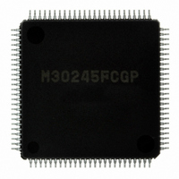
M30245FCGP#U1 Renesas Electronics America, M30245FCGP#U1 Datasheet - Page 153

M30245FCGP#U1
Manufacturer Part Number
M30245FCGP#U1
Description
IC M16C/24 MCU FLSH 128K 100LQFP
Manufacturer
Renesas Electronics America
Series
M16C™ M16C/20r
Datasheet
1.M30245FCGPU1.pdf
(268 pages)
Specifications of M30245FCGP#U1
Core Processor
M16C/60
Core Size
16-Bit
Speed
16MHz
Connectivity
I²C, SPI, SSI, UART/USART, USB
Peripherals
DMA, PWM, WDT
Number Of I /o
82
Program Memory Size
128KB (128K x 8)
Program Memory Type
FLASH
Ram Size
10K x 8
Voltage - Supply (vcc/vdd)
3 V ~ 3.6 V
Data Converters
A/D 8x10b
Oscillator Type
Internal
Operating Temperature
-20°C ~ 85°C
Package / Case
100-LQFP
Package
100LQFP
Family Name
R8C
Maximum Speed
16 MHz
Operating Supply Voltage
3.3 V
Data Bus Width
16 Bit
Number Of Programmable I/os
82
Interface Type
USB/UART/I2C/SPI
On-chip Adc
8-chx10-bit
Number Of Timers
5
Lead Free Status / RoHS Status
Lead free / RoHS Compliant
Eeprom Size
-
Available stocks
Company
Part Number
Manufacturer
Quantity
Price
- Current page: 153 of 268
- Download datasheet (3Mb)
M30245 Group
Serial Interface Special Function (SPI mode)
Figure 1.110. Example of serial bus communication control using SSi input pins
Rev.2.00
REJ03B0005-0200
SPI mode related control bit
UARTi can control communications on the serial bus using the SSi input pins. The master outputting the transfer clock
transfers data to the slave inputting the transfer clock. To prevent a bus collision, the master floats the output pin of other
slaves/masters using the SSi input pins. Figure 1.110 shows the SSi input pin factors between the master and slave.
Slave mode (STxDi and SRxDi are selected, DINC="1")
Master mode (TxDi and RxDi are selected, DINC="0")
UARTi Special Mode Register 3 (UiSMR3)
Bit 0 is the SS port function enable bit. Set this bit to "1" to enable the slave select output.
Bit 1 is the clock phase set bit.
Bit 2 is the serial input port set bit.
Bit 4 is the fault error flag. When this bit is "1", a fault error has been detected.
Bit 3, 5 to 7 : Not used in SPI mode.
When an "H" level signal is input to an SSi input pin, the STxDi and SRxDi pins both become high impedance and the
clock input is ignored. When an "L" level signal is input to an input pin, SSi clock input becomes effective and serial
communications are enabled.
The SSi input pins are used with a multiple master system. When an SSi input pin is "H" level, transmission has priority
and serial communications are enabled. When an "L" signal is input to an SSi input pin, another master exists, and the
TxDi, RxDi and CLKi pins become high impedance and the trouble error interrupt request bit becomes "1". Communi-
cations do not stop when a trouble error is generated during communications. To stop communications, set bit 0, 1, 2
of the UARTi transmit/receive mode register (addresses 03A8
Oct 16, 2006
page 151 of 264
M30245 (M)
M :Master
S :Slave
IC1
P7
P7
P7
P7
5(
6(
4(
7(
RxD
CLK
TxD
SS
P1
P1
3
3
3
3
3
2
)
)
)
)
16
, 0368
Serial Interface Special Function (SPI mode)
P7
P7
P7
P7
P7
P7
P7
P7
16
7(
6(
4(
7(
6(
4(
5(
5(
M30245 (S)
M30245 (S)
SS
CLK
SRxD
SS
CLK
SRxD
STxD
STxD
, 0338
3
3
IC2
IC3
)
)
3
3
)
)
3
3
3
3
)
)
)
)
16
, and 0328
16
) to "0".
Related parts for M30245FCGP#U1
Image
Part Number
Description
Manufacturer
Datasheet
Request
R

Part Number:
Description:
KIT STARTER FOR M16C/29
Manufacturer:
Renesas Electronics America
Datasheet:

Part Number:
Description:
KIT STARTER FOR R8C/2D
Manufacturer:
Renesas Electronics America
Datasheet:

Part Number:
Description:
R0K33062P STARTER KIT
Manufacturer:
Renesas Electronics America
Datasheet:

Part Number:
Description:
KIT STARTER FOR R8C/23 E8A
Manufacturer:
Renesas Electronics America
Datasheet:

Part Number:
Description:
KIT STARTER FOR R8C/25
Manufacturer:
Renesas Electronics America
Datasheet:

Part Number:
Description:
KIT STARTER H8S2456 SHARPE DSPLY
Manufacturer:
Renesas Electronics America
Datasheet:

Part Number:
Description:
KIT STARTER FOR R8C38C
Manufacturer:
Renesas Electronics America
Datasheet:

Part Number:
Description:
KIT STARTER FOR R8C35C
Manufacturer:
Renesas Electronics America
Datasheet:

Part Number:
Description:
KIT STARTER FOR R8CL3AC+LCD APPS
Manufacturer:
Renesas Electronics America
Datasheet:

Part Number:
Description:
KIT STARTER FOR RX610
Manufacturer:
Renesas Electronics America
Datasheet:

Part Number:
Description:
KIT STARTER FOR R32C/118
Manufacturer:
Renesas Electronics America
Datasheet:

Part Number:
Description:
KIT DEV RSK-R8C/26-29
Manufacturer:
Renesas Electronics America
Datasheet:

Part Number:
Description:
KIT STARTER FOR SH7124
Manufacturer:
Renesas Electronics America
Datasheet:

Part Number:
Description:
KIT STARTER FOR H8SX/1622
Manufacturer:
Renesas Electronics America
Datasheet:


