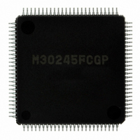
M30245FCGP#U1 Renesas Electronics America, M30245FCGP#U1 Datasheet - Page 191

M30245FCGP#U1
Manufacturer Part Number
M30245FCGP#U1
Description
IC M16C/24 MCU FLSH 128K 100LQFP
Manufacturer
Renesas Electronics America
Series
M16C™ M16C/20r
Datasheet
1.M30245FCGPU1.pdf
(268 pages)
Specifications of M30245FCGP#U1
Core Processor
M16C/60
Core Size
16-Bit
Speed
16MHz
Connectivity
I²C, SPI, SSI, UART/USART, USB
Peripherals
DMA, PWM, WDT
Number Of I /o
82
Program Memory Size
128KB (128K x 8)
Program Memory Type
FLASH
Ram Size
10K x 8
Voltage - Supply (vcc/vdd)
3 V ~ 3.6 V
Data Converters
A/D 8x10b
Oscillator Type
Internal
Operating Temperature
-20°C ~ 85°C
Package / Case
100-LQFP
Package
100LQFP
Family Name
R8C
Maximum Speed
16 MHz
Operating Supply Voltage
3.3 V
Data Bus Width
16 Bit
Number Of Programmable I/os
82
Interface Type
USB/UART/I2C/SPI
On-chip Adc
8-chx10-bit
Number Of Timers
5
Lead Free Status / RoHS Status
Lead free / RoHS Compliant
Eeprom Size
-
Available stocks
Company
Part Number
Manufacturer
Quantity
Price
- Current page: 191 of 268
- Download datasheet (3Mb)
M30245 Group
Table 1.65. Example connection of unused pins in memory expansion mode
Rev.2.00
REJ03B0005-0200
Note 1: With external clock input to X
Note 2: VbusDTCT pin is pulled down internaly.
Figure 1.142. Example connection of unused pins
P6 to P10 (excluding P8
P4
BHE, ALE, HLDA, X
HOLD, RDY, NMI
UVcc, AVcc
AVss, V
USB D+, USB D-, LPF, VbusDTCT (Note 2)
Precautions
5
/CS1 to P4
Dedicated Input Pins
If a dedicated input pin is connected to a power supply different from the supply that Vcc is connected to, a resistor
(approximately 1k ohm) should be added between the input pin and the connected power supply. However, if the
dedicated input pin voltage is higher than Vcc, latch up could occur. A resistor is not required when using a Vcc
voltage equal or greater than the voltage of the dedicated input pin.
REF
Pin name
Oct 16, 2006
, BYTE
7
/CS3
Note : When the BCLK output disable bit (bit 7 at address 0004
In single-chip mode
Port P0 to P10 (except for P8
OUT
Microcomputer
5
(Note 1), BCLK
)
USB D+, USB D-
page 189 of 264
(Output mode)
(Input mode)
(Input mode)
UVcc, AVcc
VbusDTCT
.
.
.
BYTE
X
AV
V
NMI
LPF
OUT
REF
SS
5
)
IN
pin.
Open
Open
Open
Open
Open
Vcc
.
.
.
Vcc
After setting to input mode, connect every pin to Vss or Vcc using a resistor.
OR
Leave these pins open after setting to output mode.
Set ports to input mode, set bits CS1 to CS3 to "0" (chip select disabled),
connect to Vcc using resistors (pull-up)
Open
Connect using a resistor to Vcc (pull-up)
Connect to Vcc
Connect to Vss
Open
V
SS
Vcc
16
In memory expansion mode or
in microprocessor mode
Port P4
to P4
Port P6 to P10 (except for P8
) is set to "1", connect to V
Microcomputer
7
/ CS3
5
/ CS1
USB D+, USB D-
(Output mode)
BCLK (Note)
UVcc, AVcc
(Input mode)
(Input mode)
VbusDTCT
Connection
.
.
.
HOLD
HLDA
AV
X
V
RDY
BHE
NMI
ALE
LPF
OUT
REF
SS
5
)
CC
using a pull-up resistor.
Open
Open
Open
Open
Open
.
. .
V
CC
Vcc
Programmable I/O Ports
V
SS
Related parts for M30245FCGP#U1
Image
Part Number
Description
Manufacturer
Datasheet
Request
R

Part Number:
Description:
KIT STARTER FOR M16C/29
Manufacturer:
Renesas Electronics America
Datasheet:

Part Number:
Description:
KIT STARTER FOR R8C/2D
Manufacturer:
Renesas Electronics America
Datasheet:

Part Number:
Description:
R0K33062P STARTER KIT
Manufacturer:
Renesas Electronics America
Datasheet:

Part Number:
Description:
KIT STARTER FOR R8C/23 E8A
Manufacturer:
Renesas Electronics America
Datasheet:

Part Number:
Description:
KIT STARTER FOR R8C/25
Manufacturer:
Renesas Electronics America
Datasheet:

Part Number:
Description:
KIT STARTER H8S2456 SHARPE DSPLY
Manufacturer:
Renesas Electronics America
Datasheet:

Part Number:
Description:
KIT STARTER FOR R8C38C
Manufacturer:
Renesas Electronics America
Datasheet:

Part Number:
Description:
KIT STARTER FOR R8C35C
Manufacturer:
Renesas Electronics America
Datasheet:

Part Number:
Description:
KIT STARTER FOR R8CL3AC+LCD APPS
Manufacturer:
Renesas Electronics America
Datasheet:

Part Number:
Description:
KIT STARTER FOR RX610
Manufacturer:
Renesas Electronics America
Datasheet:

Part Number:
Description:
KIT STARTER FOR R32C/118
Manufacturer:
Renesas Electronics America
Datasheet:

Part Number:
Description:
KIT DEV RSK-R8C/26-29
Manufacturer:
Renesas Electronics America
Datasheet:

Part Number:
Description:
KIT STARTER FOR SH7124
Manufacturer:
Renesas Electronics America
Datasheet:

Part Number:
Description:
KIT STARTER FOR H8SX/1622
Manufacturer:
Renesas Electronics America
Datasheet:


