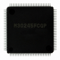
M30245FCGP#U1 Renesas Electronics America, M30245FCGP#U1 Datasheet - Page 150

M30245FCGP#U1
Manufacturer Part Number
M30245FCGP#U1
Description
IC M16C/24 MCU FLSH 128K 100LQFP
Manufacturer
Renesas Electronics America
Series
M16C™ M16C/20r
Datasheet
1.M30245FCGPU1.pdf
(268 pages)
Specifications of M30245FCGP#U1
Core Processor
M16C/60
Core Size
16-Bit
Speed
16MHz
Connectivity
I²C, SPI, SSI, UART/USART, USB
Peripherals
DMA, PWM, WDT
Number Of I /o
82
Program Memory Size
128KB (128K x 8)
Program Memory Type
FLASH
Ram Size
10K x 8
Voltage - Supply (vcc/vdd)
3 V ~ 3.6 V
Data Converters
A/D 8x10b
Oscillator Type
Internal
Operating Temperature
-20°C ~ 85°C
Package / Case
100-LQFP
Package
100LQFP
Family Name
R8C
Maximum Speed
16 MHz
Operating Supply Voltage
3.3 V
Data Bus Width
16 Bit
Number Of Programmable I/os
82
Interface Type
USB/UART/I2C/SPI
On-chip Adc
8-chx10-bit
Number Of Timers
5
Lead Free Status / RoHS Status
Lead free / RoHS Compliant
Eeprom Size
-
Available stocks
Company
Part Number
Manufacturer
Quantity
Price
- Current page: 150 of 268
- Download datasheet (3Mb)
M30245 Group
Table 1.50. Functions changed by I
Rev.2.00
REJ03B0005-0200
Figure 1.107. Start/stop condition detect timing characteristics
Interrupt numbers 13, 15, 17, 19
factor
Interrupt number 2, 8, 10, 21 factor
DMA factor
Data transfer timing from UART
receive shift register to receive buffer
UART receive/ACK interrupt request
generation timing
UARTi Special Mode Register 2 (UiSMR2)
Bit 0 is the I
and stop condition detection timing characteristics are shown in Figure 1.107.
Bit 1 is the clock synchronizing bit. When this bit is set to "1", if the falling edge is detected at pin SCLi while the internal
SCL is "H", the internal SCL is changed to "L", the baud rate generator value is reloaded and the L sector count starts.
Also, while the SCLi pin is "L", if the internal SCL changes from "L" to "H", baud rate generator stops counting. If the SCLi
pin is "H", counting restarts. Because of this function, the UARTi transmit/receive clock takes the AND condition for the
internal SCL and SCLi pin signals. This function operates from the clock half period before the first rise of the UARTi
clock to the 9th rise. To use this function, select the internal clock as the transfer clock.
Bit 2 is the SCL wait output bit. When this bit is set to "1", output from the SCLi pin is fixed to "L" at the clock's 9th fall.
When set to "0", the "L" output lock is released. This bit is unavailable when SCLi is external clock.
Bit 3 is the SDA output stop bit. When this bit is set to "1", an arbitration lost generated. If the arbitration lost detection flag
is "1", the SDAi pin simultaneously becomes high impedance.
Bit 4 is the UARTi initialize bit. While this bit is set to "1", the following operations are performed when the start condition
is detected.
shift register. Transmission starts with the first bit of the next input clock. However, the UARTi output value does not
change when the start condition is detected. It also doesn't change when the clock is input and when the first bit of data
is output.
• The receive shift register is initialized and reception starts with the first bit of the next input clock.
• The SCL wait output is set to "1". The SCLi pin becomes "L" level at the fall of the 9th bit of the clock.
• The transmit shift register is initialized and the content of the transmission register is transmitted to the transmission
Oct 16, 2006
Function
2
C mode select bit 2. Table 1.50 lists the control changes by bit when the I
page 148 of 264
3 to 6 cyles < set up time (Note)
3 to 6 cycles < hold time (Note)
Note: Cycle number shows main clock input oscillation frequency f(Xin) cycle number.
(Start condition)
(Stop condition)
2
SCL
SDA
SDA
C mode select bit 2
Acknowledge not detected (NACK)
Acknowledge detected (ACK)
Acknowledge detected (ACK)
Rising edge of the last bit of receive
clock
Rising edge of the last bit of receive
clock
Set up time
IICM2=0
Hold time
UARTi transfer (rising edge of the
last bit)
UARTi receive (falling edge of the
last bit)
UARTi receive (falling edge of the
last bit)
Rising edge of the last bit of receive
clock
Rising edge of the last bit of receive
clock
2
C mode select bit is "1". Start
I
2
C Bus interface mode
IICM2=1
Related parts for M30245FCGP#U1
Image
Part Number
Description
Manufacturer
Datasheet
Request
R

Part Number:
Description:
KIT STARTER FOR M16C/29
Manufacturer:
Renesas Electronics America
Datasheet:

Part Number:
Description:
KIT STARTER FOR R8C/2D
Manufacturer:
Renesas Electronics America
Datasheet:

Part Number:
Description:
R0K33062P STARTER KIT
Manufacturer:
Renesas Electronics America
Datasheet:

Part Number:
Description:
KIT STARTER FOR R8C/23 E8A
Manufacturer:
Renesas Electronics America
Datasheet:

Part Number:
Description:
KIT STARTER FOR R8C/25
Manufacturer:
Renesas Electronics America
Datasheet:

Part Number:
Description:
KIT STARTER H8S2456 SHARPE DSPLY
Manufacturer:
Renesas Electronics America
Datasheet:

Part Number:
Description:
KIT STARTER FOR R8C38C
Manufacturer:
Renesas Electronics America
Datasheet:

Part Number:
Description:
KIT STARTER FOR R8C35C
Manufacturer:
Renesas Electronics America
Datasheet:

Part Number:
Description:
KIT STARTER FOR R8CL3AC+LCD APPS
Manufacturer:
Renesas Electronics America
Datasheet:

Part Number:
Description:
KIT STARTER FOR RX610
Manufacturer:
Renesas Electronics America
Datasheet:

Part Number:
Description:
KIT STARTER FOR R32C/118
Manufacturer:
Renesas Electronics America
Datasheet:

Part Number:
Description:
KIT DEV RSK-R8C/26-29
Manufacturer:
Renesas Electronics America
Datasheet:

Part Number:
Description:
KIT STARTER FOR SH7124
Manufacturer:
Renesas Electronics America
Datasheet:

Part Number:
Description:
KIT STARTER FOR H8SX/1622
Manufacturer:
Renesas Electronics America
Datasheet:


