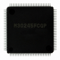
M30245FCGP#U1 Renesas Electronics America, M30245FCGP#U1 Datasheet - Page 210

M30245FCGP#U1
Manufacturer Part Number
M30245FCGP#U1
Description
IC M16C/24 MCU FLSH 128K 100LQFP
Manufacturer
Renesas Electronics America
Series
M16C™ M16C/20r
Datasheet
1.M30245FCGPU1.pdf
(268 pages)
Specifications of M30245FCGP#U1
Core Processor
M16C/60
Core Size
16-Bit
Speed
16MHz
Connectivity
I²C, SPI, SSI, UART/USART, USB
Peripherals
DMA, PWM, WDT
Number Of I /o
82
Program Memory Size
128KB (128K x 8)
Program Memory Type
FLASH
Ram Size
10K x 8
Voltage - Supply (vcc/vdd)
3 V ~ 3.6 V
Data Converters
A/D 8x10b
Oscillator Type
Internal
Operating Temperature
-20°C ~ 85°C
Package / Case
100-LQFP
Package
100LQFP
Family Name
R8C
Maximum Speed
16 MHz
Operating Supply Voltage
3.3 V
Data Bus Width
16 Bit
Number Of Programmable I/os
82
Interface Type
USB/UART/I2C/SPI
On-chip Adc
8-chx10-bit
Number Of Timers
5
Lead Free Status / RoHS Status
Lead free / RoHS Compliant
Eeprom Size
-
Available stocks
Company
Part Number
Manufacturer
Quantity
Price
- Current page: 210 of 268
- Download datasheet (3Mb)
M30245 Group
Rev.2.00
REJ03B0005-0200
Standard Serial I/O Mode
ID Code Check Function
The standard serial I/O mode serially inputs and outputs the software commands, addresses and data needed to
operate (read, program, erase, etc.) the internal flash memory. It uses a specific serial programmer to accomplish this.
It is different from the parallel I/O mode because the CPU controls operations like rewriting the flash memory (using the
CPU rewrite mode) and serially inputting data.
The standard serial I/O mode is entered by clearing the reset with the P5
set to a "L" level and the CNVss pin set to a "H" level. (For normal microprocessor mode, set the CNVss pin to "L" level.)
A control program is written in the boot ROM area when the product is shipped from Renesas. The standard serial I/O
mode cannot be used if the boot ROM area is rewritten in the parallel I/O mode. Figure 1.158 shows the pin connections
for the standard serial I/O mode. Table 1.70 lists the pin functions for standard serial IO mode.
There are two standard serial I/O modes that both require a purpose-specific serial programmer: clock synchronous
and clock asynchronous. Standard serial I/O switches between mode 1 (clock synchronous) and mode 2 (clock
asynchronous) according to the level of the CLK1 pin when the reset is released. Serial data I/O uses UART1 and
transfers the data serially in 8-bit units.
To use standard serial I/O mode 1 (clock synchronous):
• Set the CLK1 pin to "H" level and release the reset
• This mode uses the four UART1 pins CLK1, RxD1, TxD1 and RTS1 (BUSY).
• The CLK1 pin is the transfer clock input pin through which an external transfer clock is input.
• The TxD1 pin is for CMOS output.
• The RTS1 (BUSY) pin outputs an "L" level when ready for reception and an "H" level when reception starts.
To use standard serial I/O mode 2 (clock asynchronous):
• Set the CLK1 pin to "L" level and release the reset.
• This mode uses the two UART1 pins RxD1 and TxD1.
In standard serial I/O mode, only the user ROM area indicated in Figure 1.149 can be rewritten. The boot ROM cannot.
The standard serial I/O mode uses a 7-byte ID code. When there is data in the flash memory, commands sent from the
programmer are not accepted unless the ID codes are identical.
The ID code check function can be used in serial I/O mode to protect the contents of the flash memory from being read
out or rewritten. If the contents of the flash memory are not blank, the ID code sent from the serial programmer is
compared with the ID code written in the flash. If the ID codes are not identical, the commands sent from the serial
programmer are not accepted. Figure 1.159 shows the ID code store addresses. The ID code consists of 8-bit data:
(beginning with the first byte) 0FFFDF
a program that has the ID code preset at these addresses.
Oct 16, 2006
_________
page 208 of 264
16
, 0FFFE3
16
, 0FFFEB
16
, 0FFFEF
_________
16
0
, 0FFFF3
(CE) pin set to a "H" level, the P5
_____
16
, 0FFFF7
16
, and 0FFFFB
Serial I/O Mode
5
(EPM) pin
_______
16
. Write
Related parts for M30245FCGP#U1
Image
Part Number
Description
Manufacturer
Datasheet
Request
R

Part Number:
Description:
KIT STARTER FOR M16C/29
Manufacturer:
Renesas Electronics America
Datasheet:

Part Number:
Description:
KIT STARTER FOR R8C/2D
Manufacturer:
Renesas Electronics America
Datasheet:

Part Number:
Description:
R0K33062P STARTER KIT
Manufacturer:
Renesas Electronics America
Datasheet:

Part Number:
Description:
KIT STARTER FOR R8C/23 E8A
Manufacturer:
Renesas Electronics America
Datasheet:

Part Number:
Description:
KIT STARTER FOR R8C/25
Manufacturer:
Renesas Electronics America
Datasheet:

Part Number:
Description:
KIT STARTER H8S2456 SHARPE DSPLY
Manufacturer:
Renesas Electronics America
Datasheet:

Part Number:
Description:
KIT STARTER FOR R8C38C
Manufacturer:
Renesas Electronics America
Datasheet:

Part Number:
Description:
KIT STARTER FOR R8C35C
Manufacturer:
Renesas Electronics America
Datasheet:

Part Number:
Description:
KIT STARTER FOR R8CL3AC+LCD APPS
Manufacturer:
Renesas Electronics America
Datasheet:

Part Number:
Description:
KIT STARTER FOR RX610
Manufacturer:
Renesas Electronics America
Datasheet:

Part Number:
Description:
KIT STARTER FOR R32C/118
Manufacturer:
Renesas Electronics America
Datasheet:

Part Number:
Description:
KIT DEV RSK-R8C/26-29
Manufacturer:
Renesas Electronics America
Datasheet:

Part Number:
Description:
KIT STARTER FOR SH7124
Manufacturer:
Renesas Electronics America
Datasheet:

Part Number:
Description:
KIT STARTER FOR H8SX/1622
Manufacturer:
Renesas Electronics America
Datasheet:


