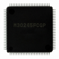
M30245FCGP#U1 Renesas Electronics America, M30245FCGP#U1 Datasheet - Page 49

M30245FCGP#U1
Manufacturer Part Number
M30245FCGP#U1
Description
IC M16C/24 MCU FLSH 128K 100LQFP
Manufacturer
Renesas Electronics America
Series
M16C™ M16C/20r
Datasheet
1.M30245FCGPU1.pdf
(268 pages)
Specifications of M30245FCGP#U1
Core Processor
M16C/60
Core Size
16-Bit
Speed
16MHz
Connectivity
I²C, SPI, SSI, UART/USART, USB
Peripherals
DMA, PWM, WDT
Number Of I /o
82
Program Memory Size
128KB (128K x 8)
Program Memory Type
FLASH
Ram Size
10K x 8
Voltage - Supply (vcc/vdd)
3 V ~ 3.6 V
Data Converters
A/D 8x10b
Oscillator Type
Internal
Operating Temperature
-20°C ~ 85°C
Package / Case
100-LQFP
Package
100LQFP
Family Name
R8C
Maximum Speed
16 MHz
Operating Supply Voltage
3.3 V
Data Bus Width
16 Bit
Number Of Programmable I/os
82
Interface Type
USB/UART/I2C/SPI
On-chip Adc
8-chx10-bit
Number Of Timers
5
Lead Free Status / RoHS Status
Lead free / RoHS Compliant
Eeprom Size
-
Available stocks
Company
Part Number
Manufacturer
Quantity
Price
- Current page: 49 of 268
- Download datasheet (3Mb)
M30245 Group
Rev.2.00
REJ03B0005-0200
Figure 1.23. Frequency Synthesizer Circuit
Frequency synthesizer circuit
Note: None of the registers must be written to once the frequency synthesizer is enabled and used as the system
The frequency synthesizer circuit generates a 48MHz clock (f
are a multiple of the external input reference clock f(X
The frequency synthesizer consists of a prescaler, frequency multiplier, a frequency divider, and five registers:
FSP; FSM; FSC; FSD; and FSCCR. Clock f(X
by FSM to generate an f
optimized for 48 MHz operation and is buffered and sent out of the frequency synthesizer block as signal fUSB.
This signal is used by the USB block.
The FSC0 bit in the FSC Control Register enables the frequency synthesizer block. When disabled (FSC0 = "0"),
f
status (LS ="1") indicates that f
Control register are shown in Figure 1.24.
When using the frequency synthesizer, a low-pass filter must be connected to the LPF pin. Once the frequency
synthesizer is enabled, a delay of 2-5ms is recommended before the output of the frequency synthesizer is
used. This is done to allow the output to stabilize. It is also recommended that none of the registers be modified
once the frequency synthesizer is enabled as it will cause the output to be temporarily (2-5ms) unstable.
The MCU clock source is selected via the Frequency Synthesizer Clock Control register (FSCCR). See Figure
1.25.
VCO
is held at either a high or low state. When the frequency synthesizer control bit is active (FSC0 = "1"), a lock
Oct 16, 2006
clock source (FSCCR register, address 03DB
to freeze. Switch system back to f(X
f(Xin)
page 47 of 264
03DE
VCO
Prescaler
FSP
clock, which is then divided by FSD to produce the clock f
SYN
f
and f
PIN
03DD
FSM
Frequency
VCO
Multiplier
IN
are the correct frequency. The LS and FSCO control bits in the FSC
) and disable before modifying PLL registers.
IN
) is prescaled down using FSP to generate f
16
03DC
f
, bit '0' set to '1') because it will cause the output of the PLL
VCO
LS
IN
FSC
). A block diagram of the circuit is shown in Figure 1.23.
USB)
Frequency
Divider
needed by the USB block and a clock f
03DF
USBC5
EN
FSD
8 Bit
Data Bus
f
SYN
f
USB
03DB
FSCCR
Frequency Synthesizer Circuit
FSCCR0
SYN
PIN
. The f
. f
PIN
VCO
is multiplied
SYN
clock is
that
Related parts for M30245FCGP#U1
Image
Part Number
Description
Manufacturer
Datasheet
Request
R

Part Number:
Description:
KIT STARTER FOR M16C/29
Manufacturer:
Renesas Electronics America
Datasheet:

Part Number:
Description:
KIT STARTER FOR R8C/2D
Manufacturer:
Renesas Electronics America
Datasheet:

Part Number:
Description:
R0K33062P STARTER KIT
Manufacturer:
Renesas Electronics America
Datasheet:

Part Number:
Description:
KIT STARTER FOR R8C/23 E8A
Manufacturer:
Renesas Electronics America
Datasheet:

Part Number:
Description:
KIT STARTER FOR R8C/25
Manufacturer:
Renesas Electronics America
Datasheet:

Part Number:
Description:
KIT STARTER H8S2456 SHARPE DSPLY
Manufacturer:
Renesas Electronics America
Datasheet:

Part Number:
Description:
KIT STARTER FOR R8C38C
Manufacturer:
Renesas Electronics America
Datasheet:

Part Number:
Description:
KIT STARTER FOR R8C35C
Manufacturer:
Renesas Electronics America
Datasheet:

Part Number:
Description:
KIT STARTER FOR R8CL3AC+LCD APPS
Manufacturer:
Renesas Electronics America
Datasheet:

Part Number:
Description:
KIT STARTER FOR RX610
Manufacturer:
Renesas Electronics America
Datasheet:

Part Number:
Description:
KIT STARTER FOR R32C/118
Manufacturer:
Renesas Electronics America
Datasheet:

Part Number:
Description:
KIT DEV RSK-R8C/26-29
Manufacturer:
Renesas Electronics America
Datasheet:

Part Number:
Description:
KIT STARTER FOR SH7124
Manufacturer:
Renesas Electronics America
Datasheet:

Part Number:
Description:
KIT STARTER FOR H8SX/1622
Manufacturer:
Renesas Electronics America
Datasheet:


