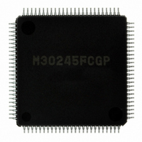
M30245FCGP#U1 Renesas Electronics America, M30245FCGP#U1 Datasheet - Page 20

M30245FCGP#U1
Manufacturer Part Number
M30245FCGP#U1
Description
IC M16C/24 MCU FLSH 128K 100LQFP
Manufacturer
Renesas Electronics America
Series
M16C™ M16C/20r
Datasheet
1.M30245FCGPU1.pdf
(268 pages)
Specifications of M30245FCGP#U1
Core Processor
M16C/60
Core Size
16-Bit
Speed
16MHz
Connectivity
I²C, SPI, SSI, UART/USART, USB
Peripherals
DMA, PWM, WDT
Number Of I /o
82
Program Memory Size
128KB (128K x 8)
Program Memory Type
FLASH
Ram Size
10K x 8
Voltage - Supply (vcc/vdd)
3 V ~ 3.6 V
Data Converters
A/D 8x10b
Oscillator Type
Internal
Operating Temperature
-20°C ~ 85°C
Package / Case
100-LQFP
Package
100LQFP
Family Name
R8C
Maximum Speed
16 MHz
Operating Supply Voltage
3.3 V
Data Bus Width
16 Bit
Number Of Programmable I/os
82
Interface Type
USB/UART/I2C/SPI
On-chip Adc
8-chx10-bit
Number Of Timers
5
Lead Free Status / RoHS Status
Lead free / RoHS Compliant
Eeprom Size
-
Available stocks
Company
Part Number
Manufacturer
Quantity
Price
- Current page: 20 of 268
- Download datasheet (3Mb)
M30245 Group
Rev.2.00
REJ03B0005-0200
Table 1.6. SFR Map (1)
Special Function Registers
Tables 1.6 to 1.13 show the peripheral control registers, their addresses, names, acronyms, and values after
reset.
Oct 16, 2006
Note 1: The contents of other registers and RAM is undefined when the microcomputer is reset. The initial value must therefore be set.
Note 2: Locations in the SFR area where nothing is assigned are reserved areas. Do not access these areas for read or write.
Note 3: For hardware reset, when Vcc is applied to the CNVss pin, it is 03
Address
000C
000D
001C
001D
002C
002D
003C
000A
000B
000E
001A
001B
001E
002A
002B
002E
003A
003B
0000
0001
0002
0003
0004
0005
0006
0007
0008
0009
000F
0010
0012
0013
0014
0015
0016
0017
0018
0019
001F
0020
0021
0022
0023
0024
0025
0026
0027
0028
0029
002F
0030
0031
0032
0033
0034
0035
0036
0037
0038
0039
0011
are preserved as before the reset.
16
16
16
16
16
16
16
16
16
16
16
16
16
16
16
16
16
16
16
16
16
16
16
16
16
16
16
16
16
16
16
16
16
16
16
16
16
16
16
16
16
16
16
16
16
16
16
16
16
16
16
16
16
16
16
16
16
16
16
16
16
Processor mode register 0 (Note 3)
Processor mode register 1
System clock control register 0
System clock control register 1
Chip select control register
Address match interrupt enable register
Protect register
USB control register
Watchdog timer start register
Watchdog timer control register
Address match interrupt register 0
Address match interrupt register 1
Chip select expansion register
Reserved
USB Attach/Detach register
DMA0 source pointer
DMA0 destination pointer
DMA0 transfer counter
DMA0 control register
DMA1 source pointer
DMA1 destination pointer
DMA1 transfer counter
DMA1 control register
page 18 of 264
Register name
Acronym
PM0
PM1
CM0
CM1
CSR
AIER
PRCR
USBC
WDTS
WDC
RMAD0
RMAD1
CSE
USBAD
SAR0
DAR0
TCR0
DM0CON
SAR1
DAR1
TCR1
DM1CON
16
at reset. For software reset, the contents of bit 0 and 1
0 0
0 0 0 0 0 0 0 1
0 0 0 ? ? ? ? ?
0 0 0 0 0 ? 0 0
0 0 0 0 0 ? 0 0
Value after reset
00
48
20
00
00
00
00
00
00
00
16
16
16
16
16
16
16
16
16
16
0 0 0 0
0 0 0 0
0 0 0
0 0
0
? :
Undefined
:
to this bit
Special Function Registers
Nothing is mapped
Related parts for M30245FCGP#U1
Image
Part Number
Description
Manufacturer
Datasheet
Request
R

Part Number:
Description:
KIT STARTER FOR M16C/29
Manufacturer:
Renesas Electronics America
Datasheet:

Part Number:
Description:
KIT STARTER FOR R8C/2D
Manufacturer:
Renesas Electronics America
Datasheet:

Part Number:
Description:
R0K33062P STARTER KIT
Manufacturer:
Renesas Electronics America
Datasheet:

Part Number:
Description:
KIT STARTER FOR R8C/23 E8A
Manufacturer:
Renesas Electronics America
Datasheet:

Part Number:
Description:
KIT STARTER FOR R8C/25
Manufacturer:
Renesas Electronics America
Datasheet:

Part Number:
Description:
KIT STARTER H8S2456 SHARPE DSPLY
Manufacturer:
Renesas Electronics America
Datasheet:

Part Number:
Description:
KIT STARTER FOR R8C38C
Manufacturer:
Renesas Electronics America
Datasheet:

Part Number:
Description:
KIT STARTER FOR R8C35C
Manufacturer:
Renesas Electronics America
Datasheet:

Part Number:
Description:
KIT STARTER FOR R8CL3AC+LCD APPS
Manufacturer:
Renesas Electronics America
Datasheet:

Part Number:
Description:
KIT STARTER FOR RX610
Manufacturer:
Renesas Electronics America
Datasheet:

Part Number:
Description:
KIT STARTER FOR R32C/118
Manufacturer:
Renesas Electronics America
Datasheet:

Part Number:
Description:
KIT DEV RSK-R8C/26-29
Manufacturer:
Renesas Electronics America
Datasheet:

Part Number:
Description:
KIT STARTER FOR SH7124
Manufacturer:
Renesas Electronics America
Datasheet:

Part Number:
Description:
KIT STARTER FOR H8SX/1622
Manufacturer:
Renesas Electronics America
Datasheet:


