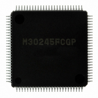
M30245FCGP#U1 Renesas Electronics America, M30245FCGP#U1 Datasheet - Page 92

M30245FCGP#U1
Manufacturer Part Number
M30245FCGP#U1
Description
IC M16C/24 MCU FLSH 128K 100LQFP
Manufacturer
Renesas Electronics America
Series
M16C™ M16C/20r
Datasheet
1.M30245FCGPU1.pdf
(268 pages)
Specifications of M30245FCGP#U1
Core Processor
M16C/60
Core Size
16-Bit
Speed
16MHz
Connectivity
I²C, SPI, SSI, UART/USART, USB
Peripherals
DMA, PWM, WDT
Number Of I /o
82
Program Memory Size
128KB (128K x 8)
Program Memory Type
FLASH
Ram Size
10K x 8
Voltage - Supply (vcc/vdd)
3 V ~ 3.6 V
Data Converters
A/D 8x10b
Oscillator Type
Internal
Operating Temperature
-20°C ~ 85°C
Package / Case
100-LQFP
Package
100LQFP
Family Name
R8C
Maximum Speed
16 MHz
Operating Supply Voltage
3.3 V
Data Bus Width
16 Bit
Number Of Programmable I/os
82
Interface Type
USB/UART/I2C/SPI
On-chip Adc
8-chx10-bit
Number Of Timers
5
Lead Free Status / RoHS Status
Lead free / RoHS Compliant
Eeprom Size
-
Available stocks
Company
Part Number
Manufacturer
Quantity
Price
- Current page: 92 of 268
- Download datasheet (3Mb)
M30245 Group
Figure 1.57. USB Endpoint 0 write count register (EP0WC)
Rev.2.00
REJ03B0005-0200
USB Endpoint 0 WRT CNT Register
USB Endpoint x IN CSR (x = 1 to 4)
USB Endpoint 0 Write Count register
(b15)
0
The USB Endpoint 0 WRT CNT Register, shown in Figure 1.57, contains the number of bytes of the current data set in
the OUT buffer. The USB FCU sets the value in the WRT_CNT Register after having successfully received a data set
from the host. The CPU reads the register to determine the number of bytes to be read from the buffer. The WRT_CNT
value does not decrement upon a CPU read from the FIFO Data Register. The WRT_CNT value is cleared when the
CPU writes a "1" to the CLR_OUT_BUF_RDY bit of the EP0 CSR.
The USB Endpoint x IN control status register, shown in Figure 1.58, contains control and status information of the
respective IN EP 1-4.
• INxCSR0 (IN_BUF_STS0) and INxCSR1 (IN_BUF_STS1):
Two status flags, indicate the current status of the IN buffer. These two flags are "1"s after reset, and become "0"s when
the respective endpoint is enabled from a disabled state. The buffer status flags get updated when one of the following
events occurs:
1. The USB FCU successfully sends out a data set to the host.
2. The CPU loads a data set to the buffer (writes a "1" to SET_IN_BUF_RDY).
3. The CPU writes a "1" to the FLUSH bit or a hardware auto flush takes place.
• INxCSR2 (UNDER_RUN):
A status flag, "1" indicates an under run has occurred in an isochronous data transfer. The USB FCU updates this flag
to a "1" at the beginning of an IN token if no data packet is in the buffer.
• INxCSR3 (SET_IN_BUF_RDY):
The CPU writes a "1" to this bit after loading a data set to the buffer. The CPU can only load data to the buffer and set this
bit when INxCSR1 (IN_BUF_STS1) is a "0".
• INxCSR4 (CLR_UNDER_RUN):
The CPU writes a "1" to this bit to clear the UNDER_RUN status flag.
• INxCSR5 (TOGGLE_INIT):
The CPU writes a "1" to this bit to initialize the data sequence, force the next packet’s data PID to a DATA0 for transmis-
sion. Setting the TOGGLE_INT bit also resets the FIFO read/write pointers.
• INxCSR5 (TOGGLE_INIT):
The CPU writes a "1" to this bit to initialize the data sequence, force the next packet’s data PID to a DATA0 for transmis-
sion. Setting the TOGGLE_INT bit also resets the FIFO read/write pointers.
b7
0 0 0 0 0 0 0
Oct 16, 2006
(b8)
b0
page 90 of 264
b7
b0
Reserved
EP0WC7-0
Bit Symbol
Symbol
EP0WC
Receive byte count
Bit Name
Address
029C
16
Must always be "0"
Function
Universal Serial Bus
When reset
0000
16
R W
O X
O O
Related parts for M30245FCGP#U1
Image
Part Number
Description
Manufacturer
Datasheet
Request
R

Part Number:
Description:
KIT STARTER FOR M16C/29
Manufacturer:
Renesas Electronics America
Datasheet:

Part Number:
Description:
KIT STARTER FOR R8C/2D
Manufacturer:
Renesas Electronics America
Datasheet:

Part Number:
Description:
R0K33062P STARTER KIT
Manufacturer:
Renesas Electronics America
Datasheet:

Part Number:
Description:
KIT STARTER FOR R8C/23 E8A
Manufacturer:
Renesas Electronics America
Datasheet:

Part Number:
Description:
KIT STARTER FOR R8C/25
Manufacturer:
Renesas Electronics America
Datasheet:

Part Number:
Description:
KIT STARTER H8S2456 SHARPE DSPLY
Manufacturer:
Renesas Electronics America
Datasheet:

Part Number:
Description:
KIT STARTER FOR R8C38C
Manufacturer:
Renesas Electronics America
Datasheet:

Part Number:
Description:
KIT STARTER FOR R8C35C
Manufacturer:
Renesas Electronics America
Datasheet:

Part Number:
Description:
KIT STARTER FOR R8CL3AC+LCD APPS
Manufacturer:
Renesas Electronics America
Datasheet:

Part Number:
Description:
KIT STARTER FOR RX610
Manufacturer:
Renesas Electronics America
Datasheet:

Part Number:
Description:
KIT STARTER FOR R32C/118
Manufacturer:
Renesas Electronics America
Datasheet:

Part Number:
Description:
KIT DEV RSK-R8C/26-29
Manufacturer:
Renesas Electronics America
Datasheet:

Part Number:
Description:
KIT STARTER FOR SH7124
Manufacturer:
Renesas Electronics America
Datasheet:

Part Number:
Description:
KIT STARTER FOR H8SX/1622
Manufacturer:
Renesas Electronics America
Datasheet:


