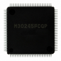
M30245FCGP#U1 Renesas Electronics America, M30245FCGP#U1 Datasheet - Page 163

M30245FCGP#U1
Manufacturer Part Number
M30245FCGP#U1
Description
IC M16C/24 MCU FLSH 128K 100LQFP
Manufacturer
Renesas Electronics America
Series
M16C™ M16C/20r
Datasheet
1.M30245FCGPU1.pdf
(268 pages)
Specifications of M30245FCGP#U1
Core Processor
M16C/60
Core Size
16-Bit
Speed
16MHz
Connectivity
I²C, SPI, SSI, UART/USART, USB
Peripherals
DMA, PWM, WDT
Number Of I /o
82
Program Memory Size
128KB (128K x 8)
Program Memory Type
FLASH
Ram Size
10K x 8
Voltage - Supply (vcc/vdd)
3 V ~ 3.6 V
Data Converters
A/D 8x10b
Oscillator Type
Internal
Operating Temperature
-20°C ~ 85°C
Package / Case
100-LQFP
Package
100LQFP
Family Name
R8C
Maximum Speed
16 MHz
Operating Supply Voltage
3.3 V
Data Bus Width
16 Bit
Number Of Programmable I/os
82
Interface Type
USB/UART/I2C/SPI
On-chip Adc
8-chx10-bit
Number Of Timers
5
Lead Free Status / RoHS Status
Lead free / RoHS Compliant
Eeprom Size
-
Available stocks
Company
Part Number
Manufacturer
Quantity
Price
M30245 Group
Rev.2.00
REJ03B0005-0200
Overview
The Serial Sound Interface is a serial data communication system. The parallel (MCU bus) to serial data conversion
is accomplished by the shift registers. Figure 1.116 shows a description of each component of the Serial Sound
Interface architecture. There are separate 32- bit shift registers for transmit and receive for full duplex operation.
Each shift register can be configured for 32, 24, or 16 bits as defined by the channel width mode bits. The shift
register loads (or stores for receiver) data from the data buffers on every WS edge. The first load and bit-shift begins
on the first "valid" edge of WS (as defined by the mode bits) after the transmit/receive mode bits are set (see Figure
1.122). Therefore, the transmit data buffers must be loaded prior to enabling the transmitter to ensure that the first
transmit contains valid data.
Both the transmitter and receiver have their own set of data buffers. There are two data buffers (left and right) so that,
on special conditions when the MCU is handling a higher priority task, additional time is available (channel width X
TSCK) before there is data underflow or overflow. The shift register always loads from or stores to the left buffer first
and alternates between the two buffers on every edge of WS. The placement of data within the buffers is described in
detail in the Data Path section.
The interrupt generator is a state machine which controls the data interface. The state machine makes the data
transfer to or from the peripheral more efficient by generating interrupts until all the data needed for the data buffer
has been accessed. The interrupt can be set up to be a DMA trigger for more efficient data transfer. The interrupt
generator also tracks the read/write width (byte/word) so that no additional control is needed. The interrupt is first
generated when a data word is loaded from the data buffer to the shift register (transmitter) or data are stored from
the shift register into the data buffer (receiver). When the MCU is finished accessing (as a response to the interrupt)
another interrupt is generated if the data buffer has not completely been accessed. For example, for a 24-bit trans-
mitter, an interrupt is generated when the left buffer is loaded into the shift register. If the MCU writes a byte of data to
the transmit buffer address, 8 of the 24 bits will be filled with new data. The interrupt generator triggers another
interrupt causing the MCU to write more data. If this write is a 16-bit operation, no further interrupts are generated
until the right buffer is loaded into the shift register. However, if the write operation is only 8 bit, then another interrupt
is generated immediately.
The data interface is used to simplify the data transfer process. The data buffer address is the same regardless of
the actual data buffer width. The interface places the incoming or outgoing data in the correct position according to
the channel width and the number of completed reads/writes for the data buffer.
The operation of the data interface is demonstrated in the example below which is the case of 24-bit audio data with
word writes. As previously explained, the state machine generates an interrupt when the left channel is loaded into
the shift register for transmission. When the first word write occurs, the data interface places the data in the left
buffer. Since 8 more bits are required to fully load the left buffer, another interrupt is generated. The MCU writes
another word of data, of which one byte is placed in the left buffer. However, the remaining data is held in a tempo-
rary buffer within the data interface since the right channel may not be loaded into the shift register yet. If the data is
not held in a temporary buffer but written to the right buffer, it would overwrite the untransmitted data in the right
buffer. When the right buffer is eventually loaded into the shift register for transmission, the state machine generates
an interrupt to request additional data. An MCU word write causes the data in the temporary buffer, as well as the
data on the MCU data bus, to be placed in the right buffer. No further interrupts are generated because all data
buffers are filled.
Oct 16, 2006
page 161 of 264
Serial Sound Interface


