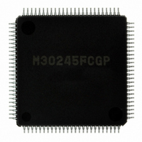
M30245FCGP#U1 Renesas Electronics America, M30245FCGP#U1 Datasheet - Page 215

M30245FCGP#U1
Manufacturer Part Number
M30245FCGP#U1
Description
IC M16C/24 MCU FLSH 128K 100LQFP
Manufacturer
Renesas Electronics America
Series
M16C™ M16C/20r
Datasheet
1.M30245FCGPU1.pdf
(268 pages)
Specifications of M30245FCGP#U1
Core Processor
M16C/60
Core Size
16-Bit
Speed
16MHz
Connectivity
I²C, SPI, SSI, UART/USART, USB
Peripherals
DMA, PWM, WDT
Number Of I /o
82
Program Memory Size
128KB (128K x 8)
Program Memory Type
FLASH
Ram Size
10K x 8
Voltage - Supply (vcc/vdd)
3 V ~ 3.6 V
Data Converters
A/D 8x10b
Oscillator Type
Internal
Operating Temperature
-20°C ~ 85°C
Package / Case
100-LQFP
Package
100LQFP
Family Name
R8C
Maximum Speed
16 MHz
Operating Supply Voltage
3.3 V
Data Bus Width
16 Bit
Number Of Programmable I/os
82
Interface Type
USB/UART/I2C/SPI
On-chip Adc
8-chx10-bit
Number Of Timers
5
Lead Free Status / RoHS Status
Lead free / RoHS Compliant
Eeprom Size
-
Available stocks
Company
Part Number
Manufacturer
Quantity
Price
- Current page: 215 of 268
- Download datasheet (3Mb)
M30245 Group
Figure 1.161. Timing for page read
Figure 1.162. Timing for the page program
Rev.2.00
REJ03B0005-0200
1. Page Read Command
The page read command reads the specified page (256 bytes) in the flash memory sequentially one byte at a time.
Figure 1.161 shows the timing for the page read.
To execute the page read command:
(1) Transfer the "FF
(2) Transfer addresses A
(3) From the 4th byte on, data (D
sequentially from the smallest address first in sync with the fall of the clock.
2. Page Program Command
This command writes the specified page (256 bytes) in the flash memory sequentially one byte at a time. Figure 1.162
shows the page program timing.
To execute the page program command:
(1) Transfer the "41
(2) Transfer addresses A
(3) From the 4th byte on, write data (D
sequentially from the smallest address first. The page is automatically written.
When reception of the page (256 bytes) ends, the RTS1 (BUSY) signal changes from the "H" to the "L" level. The status
register shows the results of the page program. Refer to the status register section for more details.
Each block is write-protected with the lock bit. Refer to the data protection function section for more details. Additional
writing of previously programmed pages is not allowed.
Oct 16, 2006
(M30245 reception data)
(M30245 transmit data)
(M30245 reception data)
(M30245 transmit data)
16
16
page 213 of 264
" command code with the 1st byte.
" command code with the 1st byte.
8
8
RTS1(BUSY)
RTS1(BUSY)
to A
to A
15
15
CLK1
RxD1
TxD1
CLK1
RxD1
TxD1
and A
and A
0
-D
7
16
16
0
) for the page (256 bytes) specified by addresses A
-D
to A
to A
7
41
) for the page (256 bytes) specified by addresses A
FF
16
23
23
16
with the 2nd and 3rd bytes respectively.
with the 2nd and 3rd bytes respectively.
_________
A
A
8
A
15
A
8
to
15
to
A
A
16
23
A
to
A
16
23
to
data0
data0
data255
data255
8
Serial I/O Mode 1
8
to A
to A
23,
23,
will be output
will be input
Related parts for M30245FCGP#U1
Image
Part Number
Description
Manufacturer
Datasheet
Request
R

Part Number:
Description:
KIT STARTER FOR M16C/29
Manufacturer:
Renesas Electronics America
Datasheet:

Part Number:
Description:
KIT STARTER FOR R8C/2D
Manufacturer:
Renesas Electronics America
Datasheet:

Part Number:
Description:
R0K33062P STARTER KIT
Manufacturer:
Renesas Electronics America
Datasheet:

Part Number:
Description:
KIT STARTER FOR R8C/23 E8A
Manufacturer:
Renesas Electronics America
Datasheet:

Part Number:
Description:
KIT STARTER FOR R8C/25
Manufacturer:
Renesas Electronics America
Datasheet:

Part Number:
Description:
KIT STARTER H8S2456 SHARPE DSPLY
Manufacturer:
Renesas Electronics America
Datasheet:

Part Number:
Description:
KIT STARTER FOR R8C38C
Manufacturer:
Renesas Electronics America
Datasheet:

Part Number:
Description:
KIT STARTER FOR R8C35C
Manufacturer:
Renesas Electronics America
Datasheet:

Part Number:
Description:
KIT STARTER FOR R8CL3AC+LCD APPS
Manufacturer:
Renesas Electronics America
Datasheet:

Part Number:
Description:
KIT STARTER FOR RX610
Manufacturer:
Renesas Electronics America
Datasheet:

Part Number:
Description:
KIT STARTER FOR R32C/118
Manufacturer:
Renesas Electronics America
Datasheet:

Part Number:
Description:
KIT DEV RSK-R8C/26-29
Manufacturer:
Renesas Electronics America
Datasheet:

Part Number:
Description:
KIT STARTER FOR SH7124
Manufacturer:
Renesas Electronics America
Datasheet:

Part Number:
Description:
KIT STARTER FOR H8SX/1622
Manufacturer:
Renesas Electronics America
Datasheet:


