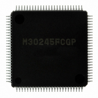
M30245FCGP#U1 Renesas Electronics America, M30245FCGP#U1 Datasheet - Page 260

M30245FCGP#U1
Manufacturer Part Number
M30245FCGP#U1
Description
IC M16C/24 MCU FLSH 128K 100LQFP
Manufacturer
Renesas Electronics America
Series
M16C™ M16C/20r
Datasheet
1.M30245FCGPU1.pdf
(268 pages)
Specifications of M30245FCGP#U1
Core Processor
M16C/60
Core Size
16-Bit
Speed
16MHz
Connectivity
I²C, SPI, SSI, UART/USART, USB
Peripherals
DMA, PWM, WDT
Number Of I /o
82
Program Memory Size
128KB (128K x 8)
Program Memory Type
FLASH
Ram Size
10K x 8
Voltage - Supply (vcc/vdd)
3 V ~ 3.6 V
Data Converters
A/D 8x10b
Oscillator Type
Internal
Operating Temperature
-20°C ~ 85°C
Package / Case
100-LQFP
Package
100LQFP
Family Name
R8C
Maximum Speed
16 MHz
Operating Supply Voltage
3.3 V
Data Bus Width
16 Bit
Number Of Programmable I/os
82
Interface Type
USB/UART/I2C/SPI
On-chip Adc
8-chx10-bit
Number Of Timers
5
Lead Free Status / RoHS Status
Lead free / RoHS Compliant
Eeprom Size
-
Available stocks
Company
Part Number
Manufacturer
Quantity
Price
- Current page: 260 of 268
- Download datasheet (3Mb)
M30245 Group
Programming Notes
Rev.2.00
REJ03B0005-0200
USB
The following Programming Notes should be incorporated into user code, to ensure strict adherence to the USB
protocol for Control Transfers.
(1) In applications requiring high-reliability, we recommend providing the system with protective measures, such as
(2) USB2.0 specification stipulates a driver impedance 28 to 44Ω (see 7.1.1.1 Full-speed (12Mb/s) Driver Characteris-
(3) Do not connect the D+ pin or the D- pin to a choke coil.
(4) If the USB Attach/Detach function will not be used, connect the UVcc pin and the USB D+ pin via a 1.5 kΩ resistor.
(5) The interrupt service routine (ISR) associated with those USB Function interrupts that are caused by errors must
Refer to the flowchart in Figure 1.211 for more information on this programming note.
USB function initialization by software or USB reset by the host, to prevent USB communication from being termi-
nated unexpectedly, for example due to external causes such as noise.
tics). Connect a serial resistor (recommended value: 27 to 33Ω) to the USB D+ pin and the USB D- pin to satisfy this
specification. Also connect, if required, a capacitor between the USB D+ pin or USB D-pin and the Vss pin. These
capacitors are to control ringing or adjust the rise and fall times and the crossover point of D+/D-. The numerical
values and configuration of the peripheral components need to be adjusted according to differences in the charac-
teristic impedance and layout of the printed circuit board. on which they are mounted. Therefore, perform careful
evaluation of the system in use and observe the waveforms before deciding on connection or disconnection and
adjusting the values of the resistors and capacitors.
(The D+ line pull-up timing depends on the UVcc pin.) If the USB Attach/Detach function is used, connect the P9
ATTACH pin and the USB D+ pin via a 1.5 kΩ resistor. Regardless of whether or not the USB Attach/Detach function
is used, connect the UVcc pin to the power supply. In addition, the time required for the host PC to recognize the USB
Attach/Detach state will vary depending state of the system as a whole, including board resistance and capacitance
components, USB cable capacitance, and the board characteristics and processing speed of the host. Perform
careful evaluation of the system in use.
have execution priority over the ISR for EP0 interrupts. Upon receipt of a USB Function interrupt, the following actions
should be taken:
Step #1: From the USB Interrupt Status (USBIS) and the USB Endpoint 0 Control & Status (EP0CS) registers,
determine if the 'Error Interrupt Status Flag' & the SETUP_END flag (i.e., INTST8 &
both set.
[YES] => Set CLR_SETUP_END (EP0CSR11). Go to Step #2.
[NO] => No special S/W action required. Go to Step #1 after the next USB Function interrupt.
Step #2: Is EP0 IN FIFO loading in progress - i.e., data has been written to EP0 IN FIFO, but SET_IN_BUF_RDY
(EP0CSR7) is not yet set?
[YES] => Set SET_IN_BUF_RDY (EP0CSR7). Go to Step #3 after the next EP0 interrupt.
[NO] => No special S/W action required. Go to Step #1 after the next USB Function interrupt.
Step #3: Are OUT_BUF_RDY & SETUP (i.e., EP0CSR0 & EP0CSR2, respectively) set?
[YES] => Go to Step #4.
[NO] => Go to Step #3 after the next EP0 interrupt.
Step #4: Does the current Control Transfer Setup stage DATA0 packet identify a Control Read Transfer?
[YES] => Complete loading EP0 IN FIFO. Set CLR_OUT_BUF_RDY, SET_IN_BUF_RDY, & CLR_SETUP (i.e.,
EP0CSR6, EP0CSR7, & EP0CSR8, respectively). Go to Step #1 after the next USB Function interrupt.
[NO] => Go to Step #3 after the next EP0 interrupt.
Oct 16, 2006
page 258 of 264
EP0CSR5, respectively) are
Usage Notes
0
/
Related parts for M30245FCGP#U1
Image
Part Number
Description
Manufacturer
Datasheet
Request
R

Part Number:
Description:
KIT STARTER FOR M16C/29
Manufacturer:
Renesas Electronics America
Datasheet:

Part Number:
Description:
KIT STARTER FOR R8C/2D
Manufacturer:
Renesas Electronics America
Datasheet:

Part Number:
Description:
R0K33062P STARTER KIT
Manufacturer:
Renesas Electronics America
Datasheet:

Part Number:
Description:
KIT STARTER FOR R8C/23 E8A
Manufacturer:
Renesas Electronics America
Datasheet:

Part Number:
Description:
KIT STARTER FOR R8C/25
Manufacturer:
Renesas Electronics America
Datasheet:

Part Number:
Description:
KIT STARTER H8S2456 SHARPE DSPLY
Manufacturer:
Renesas Electronics America
Datasheet:

Part Number:
Description:
KIT STARTER FOR R8C38C
Manufacturer:
Renesas Electronics America
Datasheet:

Part Number:
Description:
KIT STARTER FOR R8C35C
Manufacturer:
Renesas Electronics America
Datasheet:

Part Number:
Description:
KIT STARTER FOR R8CL3AC+LCD APPS
Manufacturer:
Renesas Electronics America
Datasheet:

Part Number:
Description:
KIT STARTER FOR RX610
Manufacturer:
Renesas Electronics America
Datasheet:

Part Number:
Description:
KIT STARTER FOR R32C/118
Manufacturer:
Renesas Electronics America
Datasheet:

Part Number:
Description:
KIT DEV RSK-R8C/26-29
Manufacturer:
Renesas Electronics America
Datasheet:

Part Number:
Description:
KIT STARTER FOR SH7124
Manufacturer:
Renesas Electronics America
Datasheet:

Part Number:
Description:
KIT STARTER FOR H8SX/1622
Manufacturer:
Renesas Electronics America
Datasheet:


