MOD5234-100IR NetBurner Inc, MOD5234-100IR Datasheet - Page 135
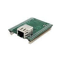
MOD5234-100IR
Manufacturer Part Number
MOD5234-100IR
Description
MOD5234 10/100 ETHERNET MODULE
Manufacturer
NetBurner Inc
Type
Controllers & Processorsr
Datasheets
1.MOD5272-100IR.pdf
(3 pages)
2.MOD5234-100IR.pdf
(4 pages)
3.MOD5234-100IR.pdf
(754 pages)
Specifications of MOD5234-100IR
Interface
I²C, SPI, UART
Voltage - Supply
2.5V
Mounting Type
Surface Mount
Package / Case
Module
Product
Modules
Lead Free Status / RoHS Status
Lead free / RoHS Compliant
Data Format
-
Baud Rates
-
Lead Free Status / Rohs Status
Lead free / RoHS Compliant
Other names
Q4483564


Freescale Semiconductor
19–11
Bits
7–6
3–2
1–0
21
20
10
9
8
5
4
DBWE
Name
EUSP
CLNF
INVD
CEIB
DCM
DWP
INVI
—
—
—
Table 5-4. CACR Field Descriptions (Continued)
CINV instruction cache only. This bit can not be set unless the cache configuration is split
(both DISI and DISD cleared). For instruction or data cache configurations this bit is a
don’t-care. For the split cache configuration, this bit is part of the control for the invalidate
all operation. See the CINV definition for a detailed description
Table 5-6
CINV data cache only. This bit can not be set unless the cache configuration is split (both
DISI and DISD cleared). For instruction or data cache configurations this bit is a don’t-care.
For the split cache configuration, this bit is part of the control for the invalidate all operation.
See the CINV definition for a detailed description
Table 5-6
Reserved, should be cleared.
Cache enable noncacheable instruction bursting. Setting this bit enables the line-fill buffer
to be loaded with burst transfers under control of CLNF[1:0] for noncacheable accesses.
Noncacheable accesses are never written into the memory array. See
0 Disable burst fetches on noncacheable accesses
1 Enable burst fetches on noncacheable accesses
Default cache mode. This bit defines the default cache mode: 0 is cacheable, 1 is
noncacheable. For more information on the selection of the effective memory attributes,
see
0 Caching enabled
1 Caching disabled
Default buffered write enable. This bit defines the default value for enabling buffered writes.
If DBWE = 0, the termination of an operand write cycle on the processor's local bus is
delayed until the external bus cycle is completed. If DBWE = 1, the write cycle on the local
bus is terminated immediately and the operation buffered in the bus controller. In this
mode, operand write cycles are effectively decoupled between the processor's local bus
and the external bus. Generally, enabled buffered writes provide higher system
performance but recovery from access errors can be more difficult. For the ColdFire core,
reporting access errors on operand writes is always imprecise and enabling buffered writes
further decouples the write instruction and the signaling of the fault
0 Disable buffered writes
1 Enable buffered writes
Reserved, should be cleared.
0 Read and write accesses permitted
1 Only read accesses permitted
Enable user stack pointer. See
OTHER_A7)," for more information on the dual stack pointer implementation.
0 Disable the processor’s use of the User Stack Pointer
1 Enable the processor’s use of the User Stack Pointer
Reserved, should be cleared.
Cache line fill. These bits control the size of the memory request the cache issues to the
bus controller for different initial instruction line access offsets. See
fetch size based on miss address and CLNF.
Default write protection
Section 5.1.3.2, “Memory Reference
describes how to set the cache invalidate all bit.
describes how to set the cache invalidate all bit.
MCF5235 Reference Manual, Rev. 2
Section 3.2.3.2, “Supervisor/User Stack Pointers (A7 and
Description
Attributes.
Memory Map/Register Definition
Table 5-1
Table
5-2.
for external
5-9
Related parts for MOD5234-100IR
Image
Part Number
Description
Manufacturer
Datasheet
Request
R

Part Number:
Description:
MCU, MPU & DSP Development Tools MOD5234 MODULE
Manufacturer:
NetBurner Inc
Datasheet:

Part Number:
Description:
MCU, MPU & DSP Development Tools MOD5234 Core Module Development Kit
Manufacturer:
NetBurner Inc
Datasheet:

Part Number:
Description:
BOARD SERIAL-ETHERNET 512K FLASH
Manufacturer:
NetBurner Inc
Datasheet:

Part Number:
Description:
PROCESSOR MODULE FLASH MOD5272
Manufacturer:
NetBurner Inc
Datasheet:

Part Number:
Description:
PROCESSOR MODULE 512KB FLASH
Manufacturer:
NetBurner Inc
Datasheet:

Part Number:
Description:
DUAL PORT SERIAL-ETHERNET
Manufacturer:
NetBurner Inc
Datasheet:

Part Number:
Description:
PROCESSOR MODULE FLASH
Manufacturer:
NetBurner Inc
Datasheet:

Part Number:
Description:
PROCESSOR MODULE 512KB FLASH
Manufacturer:
NetBurner Inc
Datasheet:

Part Number:
Description:
KIT DEVELOP NETWORK FOR MOD5282
Manufacturer:
NetBurner Inc
Datasheet:

Part Number:
Description:
KIT DEVELOP NETWORK FOR MOD5272
Manufacturer:
NetBurner Inc
Datasheet:

Part Number:
Description:
DUAL PORT SERIAL-ETHERNET
Manufacturer:
NetBurner Inc
Datasheet:

Part Number:
Description:
Ethernet Modules & Development Tools 32 Bit 66MHz 40 Pin DIP Industrial Temp
Manufacturer:
NetBurner Inc
Datasheet:

Part Number:
Description:
Ethernet ICs 32bit 147MHz CAN-to- Ethnt Device IndTemp
Manufacturer:
NetBurner Inc
Datasheet: