MOD5234-100IR NetBurner Inc, MOD5234-100IR Datasheet - Page 433
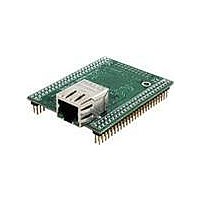
MOD5234-100IR
Manufacturer Part Number
MOD5234-100IR
Description
MOD5234 10/100 ETHERNET MODULE
Manufacturer
NetBurner Inc
Type
Controllers & Processorsr
Datasheets
1.MOD5272-100IR.pdf
(3 pages)
2.MOD5234-100IR.pdf
(4 pages)
3.MOD5234-100IR.pdf
(754 pages)
Specifications of MOD5234-100IR
Interface
I²C, SPI, UART
Voltage - Supply
2.5V
Mounting Type
Surface Mount
Package / Case
Module
Product
Modules
Lead Free Status / RoHS Status
Lead free / RoHS Compliant
Data Format
-
Baud Rates
-
Lead Free Status / Rohs Status
Lead free / RoHS Compliant
Other names
Q4483564


20.6.2.1.3 eTPU MISC Compare Register (ETPU_MISCCMPR)
ETPU_MISCCMPR holds the 32-bit signature expected from the whole shared code memory
(SCM) array. This register must be written by the host with the 32-bit word to be compared against
the calculated signature at the end of the MISC cycle. For more details, refer to the eTPU User’s
Manual.
Freescale Semiconductor
1
The parameter pointed by {CTBASE, PARM0} is the first transferred.
30–26
25–16
14–8
Bits
6–0
31
15
7
CTBASE
PBBASE
PWIDTH
PARM0
PARM1
Name
STS
WR
Table 20-4. ETPU_CDCR Field Descriptions
Start. Set by the host in order to start the data transfer between the parameter buffer
pointed by PBBASE and the target addresses selected by the concatenation of fields
CTBASE and PARM0/1. The host receives wait-states until the data transfer is complete.
Coherency logic resets STS once the data transfer is complete. For more information, refer
to the eTPU User’s Manual.
0 (Write) does not start a coherent transfer.
1 (Write) starts a coherent transfer.
Channel transfer base. This field concatenates with fields PARM0/PARM1 to determine the
absolute offset (from the SDM base) of the parameters to be transferred:
Parameter 0 address = {CTBASE, PARM0} × 4 + SDM base
Parameter 1 address = {CTBASE, PARM1} × 4 + SDM base
Parameter buffer base address. Points to the base address of the parameter buffer
location, with granularity of 2 parameters (8 bytes). The host (byte) address of the first
parameter in the buffer is PBBASE × 8 + SDM Base Address.
Parameter width selection. Selects the width of the parameters to be transferred between
the PB and the target address.
0 Transfer 24-bit parameters. The upper byte remains unchanged in the destination
1 Transfer 32-bit parameters. All 32 bits of the parameters are written in the destination
Channel Parameter number 0. This field in concatenation with CTBASE[3:0] determine the
address offset (from the SDM base address) of the parameter which is the destination or
source (defined by WR) of the coherent transfer. The SDM address offset of the parameter
is {CTBASE, PARM0}*4.Note that PARM0 allows non-contiguous parameters to be
transferred coherently
Read/Write selection. This bit selects the direction of the coherent data transfer.
0 Read operation. Data transfer is from the selected data memory address to the PB.
1 Write operation. Data transfer is from the PB to the selected data memory address.
Channel Parameter number 1. This field in concatenation with CTBASE[3:0] determines
the address offset (from the SDM base) of the parameter which is the destination or source
(defined by WR) of the coherent transfer. The SDM address offset of the parameter is
{CTBASE, PARM1}*4.Note that PARM1 allows non-contiguous parameters to be
transferred coherently
address.
address.
MCF5235 Reference Manual, Rev. 2
1
1
.
.
Description
Memory Map/Register Definition
20-19
Related parts for MOD5234-100IR
Image
Part Number
Description
Manufacturer
Datasheet
Request
R

Part Number:
Description:
MCU, MPU & DSP Development Tools MOD5234 MODULE
Manufacturer:
NetBurner Inc
Datasheet:

Part Number:
Description:
MCU, MPU & DSP Development Tools MOD5234 Core Module Development Kit
Manufacturer:
NetBurner Inc
Datasheet:

Part Number:
Description:
BOARD SERIAL-ETHERNET 512K FLASH
Manufacturer:
NetBurner Inc
Datasheet:

Part Number:
Description:
PROCESSOR MODULE FLASH MOD5272
Manufacturer:
NetBurner Inc
Datasheet:

Part Number:
Description:
PROCESSOR MODULE 512KB FLASH
Manufacturer:
NetBurner Inc
Datasheet:

Part Number:
Description:
DUAL PORT SERIAL-ETHERNET
Manufacturer:
NetBurner Inc
Datasheet:

Part Number:
Description:
PROCESSOR MODULE FLASH
Manufacturer:
NetBurner Inc
Datasheet:

Part Number:
Description:
PROCESSOR MODULE 512KB FLASH
Manufacturer:
NetBurner Inc
Datasheet:

Part Number:
Description:
KIT DEVELOP NETWORK FOR MOD5282
Manufacturer:
NetBurner Inc
Datasheet:

Part Number:
Description:
KIT DEVELOP NETWORK FOR MOD5272
Manufacturer:
NetBurner Inc
Datasheet:

Part Number:
Description:
DUAL PORT SERIAL-ETHERNET
Manufacturer:
NetBurner Inc
Datasheet:

Part Number:
Description:
Ethernet Modules & Development Tools 32 Bit 66MHz 40 Pin DIP Industrial Temp
Manufacturer:
NetBurner Inc
Datasheet:

Part Number:
Description:
Ethernet ICs 32bit 147MHz CAN-to- Ethnt Device IndTemp
Manufacturer:
NetBurner Inc
Datasheet: