MOD5234-100IR NetBurner Inc, MOD5234-100IR Datasheet - Page 642
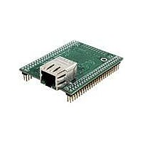
MOD5234-100IR
Manufacturer Part Number
MOD5234-100IR
Description
MOD5234 10/100 ETHERNET MODULE
Manufacturer
NetBurner Inc
Type
Controllers & Processorsr
Datasheets
1.MOD5272-100IR.pdf
(3 pages)
2.MOD5234-100IR.pdf
(4 pages)
3.MOD5234-100IR.pdf
(754 pages)
Specifications of MOD5234-100IR
Interface
I²C, SPI, UART
Voltage - Supply
2.5V
Mounting Type
Surface Mount
Package / Case
Module
Product
Modules
Lead Free Status / RoHS Status
Lead free / RoHS Compliant
Data Format
-
Baud Rates
-
Lead Free Status / Rohs Status
Lead free / RoHS Compliant
Other names
Q4483564


IEEE 1149.1 Test Access Port (JTAG)
data is accessible by shifting it through the boundary scan register to the TDO output by using the
shift-DR state. Both the data capture and the shift operation are transparent to system operation.
31.4.3.4 SAMPLE/PRELOAD Instruction
The SAMPLE/PRELOAD instruction has two functions:
31.4.3.5 ENABLE_TEST_CTRL Instruction
The ENABLE_TEST_CTRL instruction selects a 1-bit shift register (TEST_CTRL) for
connection as a shift path between the TDI and TDO pin. When the user transitions the TAP
controller to the UPDATE_DR state, the register transfers its value to a parallel hold register.
31.4.3.6 HIGHZ Instruction
The HIGHZ instruction eliminates the need to backdrive the output pins during circuit-board
testing. HIGHZ turns off all output drivers, including the 2-state drivers, and selects the bypass
register. HIGHZ also asserts internal reset for the MCU system logic to force a predictable internal
state.
31.4.3.7 CLAMP Instruction
The CLAMP instruction selects the 1-bit bypass register and asserts internal reset while
simultaneously forcing all output pins and bidirectional pins configured as outputs to the fixed
values that are preloaded and held in the boundary scan update register. CLAMP enhances test
efficiency by reducing the overall shift path to a single bit (the bypass register) while conducting
an EXTEST type of instruction through the boundary scan register.
31.4.3.8 BYPASS Instruction
The BYPASS instruction selects the bypass register, creating a single-bit shift register path from
the TDI pin to the TDO pin. BYPASS enhances test efficiency by reducing the overall shift path
31-10
• SAMPLE - See
• PRELOAD - initialize the boundary scan register update cells before selecting EXTEST or
CLAMP. This is achieved by ignoring the data shifting out on the TDO pin and shifting in
initialization data. The update-DR state and the falling edge of TCLK can then transfer this
data to the update cells. The data is applied to the external output pins by the EXTEST or
CLAMP instruction.
External synchronization is required to achieve meaningful results
because there is no internal synchronization between TCLK and the
system clock.
Section 31.4.3.3, “SAMPLE
MCF5235 Reference Manual, Rev. 2
NOTE
Instruction” for description of this function.
Freescale Semiconductor
Related parts for MOD5234-100IR
Image
Part Number
Description
Manufacturer
Datasheet
Request
R

Part Number:
Description:
MCU, MPU & DSP Development Tools MOD5234 MODULE
Manufacturer:
NetBurner Inc
Datasheet:

Part Number:
Description:
MCU, MPU & DSP Development Tools MOD5234 Core Module Development Kit
Manufacturer:
NetBurner Inc
Datasheet:

Part Number:
Description:
BOARD SERIAL-ETHERNET 512K FLASH
Manufacturer:
NetBurner Inc
Datasheet:

Part Number:
Description:
PROCESSOR MODULE FLASH MOD5272
Manufacturer:
NetBurner Inc
Datasheet:

Part Number:
Description:
PROCESSOR MODULE 512KB FLASH
Manufacturer:
NetBurner Inc
Datasheet:

Part Number:
Description:
DUAL PORT SERIAL-ETHERNET
Manufacturer:
NetBurner Inc
Datasheet:

Part Number:
Description:
PROCESSOR MODULE FLASH
Manufacturer:
NetBurner Inc
Datasheet:

Part Number:
Description:
PROCESSOR MODULE 512KB FLASH
Manufacturer:
NetBurner Inc
Datasheet:

Part Number:
Description:
KIT DEVELOP NETWORK FOR MOD5282
Manufacturer:
NetBurner Inc
Datasheet:

Part Number:
Description:
KIT DEVELOP NETWORK FOR MOD5272
Manufacturer:
NetBurner Inc
Datasheet:

Part Number:
Description:
DUAL PORT SERIAL-ETHERNET
Manufacturer:
NetBurner Inc
Datasheet:

Part Number:
Description:
Ethernet Modules & Development Tools 32 Bit 66MHz 40 Pin DIP Industrial Temp
Manufacturer:
NetBurner Inc
Datasheet:

Part Number:
Description:
Ethernet ICs 32bit 147MHz CAN-to- Ethnt Device IndTemp
Manufacturer:
NetBurner Inc
Datasheet: