MOD5234-100IR NetBurner Inc, MOD5234-100IR Datasheet - Page 288
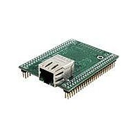
MOD5234-100IR
Manufacturer Part Number
MOD5234-100IR
Description
MOD5234 10/100 ETHERNET MODULE
Manufacturer
NetBurner Inc
Type
Controllers & Processorsr
Datasheets
1.MOD5272-100IR.pdf
(3 pages)
2.MOD5234-100IR.pdf
(4 pages)
3.MOD5234-100IR.pdf
(754 pages)
Specifications of MOD5234-100IR
Interface
I²C, SPI, UART
Voltage - Supply
2.5V
Mounting Type
Surface Mount
Package / Case
Module
Product
Modules
Lead Free Status / RoHS Status
Lead free / RoHS Compliant
Data Format
-
Baud Rates
-
Lead Free Status / Rohs Status
Lead free / RoHS Compliant
Other names
Q4483564


DMA Controller Module
Any operation involving the DMA module follows the same three steps:
14.3
This section describes each internal register and its bit assignment. Note that modifying DMA
control registers during a DMA transfer can result in undefined operation.
mapping of DMA controller registers.
14-4
1
1. Channel initialization—Channel registers are loaded with control information, address
2. Data transfer—The DMA accepts requests for operand transfers and provides addressing
3. Channel termination—Occurs after the operation is finished, either successfully or due to
Located within the SCM, but listed here for clarity.
Channel
pointers, and a byte-transfer count.
and bus control for the transfers.
an error. The channel indicates the operation status in the channel’s DSR, described in
Section 14.3.4.1, “DMA Status Registers
DMA
—
0
1
2
3
Memory Map/Register Definition
Table 14-1. Memory Map for DMA Controller Module Registers
IPSBAR Offset
0x00_011C
0x00_012C
0x00_013C
0x00_0014
0x00_0100
0x00_0104
0x00_0108
0x00_0110
0x00_0114
0x00_0118
0x00_0120
0x00_0124
0x00_0128
0x00_0130
0x00_0134
0x00_0138
0x00_010C
Status Register 0
Status Register 1
Status Register 2
Status Register 3
(DSR0)
(DSR1)
(DSR2)
(DSR3)
[31:24]
MCF5235 Reference Manual, Rev. 2
DMA Request Control Register (DMAREQC)
Destination Address Register 0 (DAR0)
Destination Address Register 1 (DAR1)
Destination Address Register 2 (DAR2)
Destination Address Register 3 (DAR3)
Source Address Register 0 (SAR0)
Source Address Register 1 (SAR1)
Source Address Register 2 (SAR2)
Source Address Register 3 (SAR3)
(DSR0–DSR3).”
[23:16]
Control Register 0 (DCR0)
Control Register 1 (DCR1)
Control Register 2 (DCR2)
Control Register 3 (DCR3)
Byte Count Register 0 (BCR0)
Byte Count Register 1 (BCR1)
Byte Count Register 2 (BCR2)
Byte Count Register 3 (BCR3)
[15:8]
Table 14-1
Freescale Semiconductor
1
[7:0]
shows the
Related parts for MOD5234-100IR
Image
Part Number
Description
Manufacturer
Datasheet
Request
R

Part Number:
Description:
MCU, MPU & DSP Development Tools MOD5234 MODULE
Manufacturer:
NetBurner Inc
Datasheet:

Part Number:
Description:
MCU, MPU & DSP Development Tools MOD5234 Core Module Development Kit
Manufacturer:
NetBurner Inc
Datasheet:

Part Number:
Description:
BOARD SERIAL-ETHERNET 512K FLASH
Manufacturer:
NetBurner Inc
Datasheet:

Part Number:
Description:
PROCESSOR MODULE FLASH MOD5272
Manufacturer:
NetBurner Inc
Datasheet:

Part Number:
Description:
PROCESSOR MODULE 512KB FLASH
Manufacturer:
NetBurner Inc
Datasheet:

Part Number:
Description:
DUAL PORT SERIAL-ETHERNET
Manufacturer:
NetBurner Inc
Datasheet:

Part Number:
Description:
PROCESSOR MODULE FLASH
Manufacturer:
NetBurner Inc
Datasheet:

Part Number:
Description:
PROCESSOR MODULE 512KB FLASH
Manufacturer:
NetBurner Inc
Datasheet:

Part Number:
Description:
KIT DEVELOP NETWORK FOR MOD5282
Manufacturer:
NetBurner Inc
Datasheet:

Part Number:
Description:
KIT DEVELOP NETWORK FOR MOD5272
Manufacturer:
NetBurner Inc
Datasheet:

Part Number:
Description:
DUAL PORT SERIAL-ETHERNET
Manufacturer:
NetBurner Inc
Datasheet:

Part Number:
Description:
Ethernet Modules & Development Tools 32 Bit 66MHz 40 Pin DIP Industrial Temp
Manufacturer:
NetBurner Inc
Datasheet:

Part Number:
Description:
Ethernet ICs 32bit 147MHz CAN-to- Ethnt Device IndTemp
Manufacturer:
NetBurner Inc
Datasheet: