MOD5234-100IR NetBurner Inc, MOD5234-100IR Datasheet - Page 637
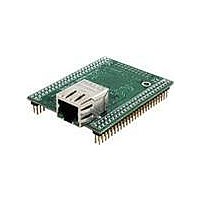
MOD5234-100IR
Manufacturer Part Number
MOD5234-100IR
Description
MOD5234 10/100 ETHERNET MODULE
Manufacturer
NetBurner Inc
Type
Controllers & Processorsr
Datasheets
1.MOD5272-100IR.pdf
(3 pages)
2.MOD5234-100IR.pdf
(4 pages)
3.MOD5234-100IR.pdf
(754 pages)
Specifications of MOD5234-100IR
Interface
I²C, SPI, UART
Voltage - Supply
2.5V
Mounting Type
Surface Mount
Package / Case
Module
Product
Modules
Lead Free Status / RoHS Status
Lead free / RoHS Compliant
Data Format
-
Baud Rates
-
Lead Free Status / Rohs Status
Lead free / RoHS Compliant
Other names
Q4483564


31.2.6 Test Data Output/Development Serial Output (TDO/DSO)
The TDO pin is the lsb-first data output. Data is clocked out of TDO on the falling edge of TCLK.
TDO is tri-stateable and is actively driven in the shift-IR and shift-DR controller states.
The DSO pin provides serial output data in BDM mode.
31.3 Memory Map/Register Definition
The JTAG module registers are not memory mapped and are only accessible through the
TDO/DSO pin.
31.3.1 Register Descriptions
All registers are shift-in and parallel load.
31.3.1.1 Instruction Shift Register (IR)
The JTAG module uses a 5-bit shift register with no parity. The IR transfers its value to a parallel
hold register and applies an instruction on the falling edge of TCLK when the TAP state machine
is in the update-IR state. To load an instruction into the shift portion of the IR, place the serial data
on the TDI pin before each rising edge of TCLK. The msb of the IR is the bit closest to the TDI
pin, and the lsb is the bit closest to the TDO pin.
31.3.1.2 IDCODE Register
The IDCODE is a read-only register; its value is chip dependent. For more information, see
Section 31.4.3.2, “IDCODE
Freescale Semiconductor
Figure 31-2. 5-Bit Instruction Register (IR)
Instruction.”
Reset
W
R
MCF5235 Reference Manual, Rev. 2
1
0
4
3
0
0
Instruction Code
1
0
2
0
0
1
1
1
0
Memory Map/Register Definition
31-5
Related parts for MOD5234-100IR
Image
Part Number
Description
Manufacturer
Datasheet
Request
R

Part Number:
Description:
MCU, MPU & DSP Development Tools MOD5234 MODULE
Manufacturer:
NetBurner Inc
Datasheet:

Part Number:
Description:
MCU, MPU & DSP Development Tools MOD5234 Core Module Development Kit
Manufacturer:
NetBurner Inc
Datasheet:

Part Number:
Description:
BOARD SERIAL-ETHERNET 512K FLASH
Manufacturer:
NetBurner Inc
Datasheet:

Part Number:
Description:
PROCESSOR MODULE FLASH MOD5272
Manufacturer:
NetBurner Inc
Datasheet:

Part Number:
Description:
PROCESSOR MODULE 512KB FLASH
Manufacturer:
NetBurner Inc
Datasheet:

Part Number:
Description:
DUAL PORT SERIAL-ETHERNET
Manufacturer:
NetBurner Inc
Datasheet:

Part Number:
Description:
PROCESSOR MODULE FLASH
Manufacturer:
NetBurner Inc
Datasheet:

Part Number:
Description:
PROCESSOR MODULE 512KB FLASH
Manufacturer:
NetBurner Inc
Datasheet:

Part Number:
Description:
KIT DEVELOP NETWORK FOR MOD5282
Manufacturer:
NetBurner Inc
Datasheet:

Part Number:
Description:
KIT DEVELOP NETWORK FOR MOD5272
Manufacturer:
NetBurner Inc
Datasheet:

Part Number:
Description:
DUAL PORT SERIAL-ETHERNET
Manufacturer:
NetBurner Inc
Datasheet:

Part Number:
Description:
Ethernet Modules & Development Tools 32 Bit 66MHz 40 Pin DIP Industrial Temp
Manufacturer:
NetBurner Inc
Datasheet:

Part Number:
Description:
Ethernet ICs 32bit 147MHz CAN-to- Ethnt Device IndTemp
Manufacturer:
NetBurner Inc
Datasheet: