MOD5234-100IR NetBurner Inc, MOD5234-100IR Datasheet - Page 342
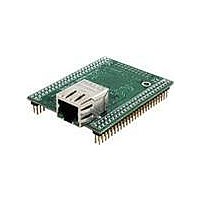
MOD5234-100IR
Manufacturer Part Number
MOD5234-100IR
Description
MOD5234 10/100 ETHERNET MODULE
Manufacturer
NetBurner Inc
Type
Controllers & Processorsr
Datasheets
1.MOD5272-100IR.pdf
(3 pages)
2.MOD5234-100IR.pdf
(4 pages)
3.MOD5234-100IR.pdf
(754 pages)
Specifications of MOD5234-100IR
Interface
I²C, SPI, UART
Voltage - Supply
2.5V
Mounting Type
Surface Mount
Package / Case
Module
Product
Modules
Lead Free Status / RoHS Status
Lead free / RoHS Compliant
Data Format
-
Baud Rates
-
Lead Free Status / Rohs Status
Lead free / RoHS Compliant
Other names
Q4483564


Synchronous DRAM Controller Module
SDRAMs operate differently than asynchronous DRAMs, particularly in the use of data pipelines
and commands to initiate special actions. Commands are issued to memory using specific
encodings on address and control pins. Soon after system reset, a command must be sent to the
SDRAM mode register to configure SDRAM operating parameters.
18.2
Table 18-2
18-4
SD_SRAS
SD_SCAS
SD_WE
SD_CS[1:0]
SD_CKE
BS[3:0]
OE
Command
WRITE
SELFX
READ
PALL
SELF
REF
Signal
External Signal Description
describes the behavior of DRAM signals in synchronous mode.
Precharge all. Precharges all internal banks of an SDRAM component; executed before new page is
opened.
Read access. SDRAM registers column address and decodes that a read access is occurring.
Refresh. Refreshes internal bank rows of an SDRAM component.
Self refresh. Refreshes internal bank rows of an SDRAM component when it is in low-power mode.
Exit self refresh. This command is sent to the DRAM controller when DCR[IS] is cleared.
Write access. SDRAM registers column address and decodes that a write access is occurring.
Synchronous row address strobe. Indicates a valid SDRAM row address is present and can be
latched by the SDRAM. SD_SRAS should be connected to the corresponding SDRAM SD_SRAS.
Synchronous column address strobe. Indicates a valid column address is present and can be
latched by the SDRAM. SD_SCAS should be connected to the corresponding SDRAM SD_SCAS.
SDRAM read/write. Asserted for write operations and negated for read operations.
Select each memory block of SDRAMs connected to the MCF5235. One SD_CS signal selects
one SDRAM block and connects to the corresponding CS signals.
Synchronous DRAM clock enable. Connected directly to the CKE (clock enable) signal of
SDRAMs. Enables and disables the clock internal to SDRAM. When CKE is deasserted, memory
can enter a power-down mode in which operations are suspended or capable of entering
self-refresh mode. SD_CKE functionality is controlled by DCR[COC]. For designs using external
multiplexing, setting COC allows SD_CKE to provide command-bit functionality.
BS[3:0] function as byte enables to the SDRAMs. They connect to the BS signals (or mask
qualifiers) of the SDRAMs.
Output Enable for SDRAM write data. During a write to the SDRAM, OE will be asserted during
the time that data is valid. This signal could be used to control the three-stating and activation of
the on-chip I/O buffers that are connected to the SDRAM data (Q) lines. This signal is low during
SDRAM reads. Do not confuse this signal with BS.
Table 18-2. Synchronous DRAM Signal Connections
Table 18-1. SDRAM Commands (Continued)
MCF5235 Reference Manual, Rev. 2
Definition
Description
Freescale Semiconductor
Related parts for MOD5234-100IR
Image
Part Number
Description
Manufacturer
Datasheet
Request
R

Part Number:
Description:
MCU, MPU & DSP Development Tools MOD5234 MODULE
Manufacturer:
NetBurner Inc
Datasheet:

Part Number:
Description:
MCU, MPU & DSP Development Tools MOD5234 Core Module Development Kit
Manufacturer:
NetBurner Inc
Datasheet:

Part Number:
Description:
BOARD SERIAL-ETHERNET 512K FLASH
Manufacturer:
NetBurner Inc
Datasheet:

Part Number:
Description:
PROCESSOR MODULE FLASH MOD5272
Manufacturer:
NetBurner Inc
Datasheet:

Part Number:
Description:
PROCESSOR MODULE 512KB FLASH
Manufacturer:
NetBurner Inc
Datasheet:

Part Number:
Description:
DUAL PORT SERIAL-ETHERNET
Manufacturer:
NetBurner Inc
Datasheet:

Part Number:
Description:
PROCESSOR MODULE FLASH
Manufacturer:
NetBurner Inc
Datasheet:

Part Number:
Description:
PROCESSOR MODULE 512KB FLASH
Manufacturer:
NetBurner Inc
Datasheet:

Part Number:
Description:
KIT DEVELOP NETWORK FOR MOD5282
Manufacturer:
NetBurner Inc
Datasheet:

Part Number:
Description:
KIT DEVELOP NETWORK FOR MOD5272
Manufacturer:
NetBurner Inc
Datasheet:

Part Number:
Description:
DUAL PORT SERIAL-ETHERNET
Manufacturer:
NetBurner Inc
Datasheet:

Part Number:
Description:
Ethernet Modules & Development Tools 32 Bit 66MHz 40 Pin DIP Industrial Temp
Manufacturer:
NetBurner Inc
Datasheet:

Part Number:
Description:
Ethernet ICs 32bit 147MHz CAN-to- Ethnt Device IndTemp
Manufacturer:
NetBurner Inc
Datasheet: