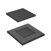
HD6417720BP133BV Renesas Electronics America, HD6417720BP133BV Datasheet - Page 1003

HD6417720BP133BV
Manufacturer Part Number
HD6417720BP133BV
Description
SH3-DSP, WITH USB AND LCDC, PB-F
Manufacturer
Renesas Electronics America
Series
SuperH® SH7700r
Datasheet
1.R8A77210C133BAV.pdf
(1478 pages)
Specifications of HD6417720BP133BV
Core Processor
SH-3 DSP
Core Size
32-Bit
Speed
133MHz
Connectivity
FIFO, I²C, IrDA, MMC, SCI, SD, SIO, SIM, USB
Peripherals
DMA, LCD, POR, WDT
Number Of I /o
117
Program Memory Type
ROMless
Ram Size
16K x 8
Voltage - Supply (vcc/vdd)
1.4 V ~ 1.6 V
Data Converters
A/D 4x10b; D/A 2x8b
Oscillator Type
Internal
Operating Temperature
-20°C ~ 75°C
Package / Case
256-BGA
Lead Free Status / RoHS Status
Lead free / RoHS Compliant
Eeprom Size
-
Program Memory Size
-
- Current page: 1003 of 1478
- Download datasheet (10Mb)
SH7720 Group, SH7721 Group
Table 27.3 A/D Conversion Time (Single Mode)
Note: Values in the table are numbers of states (t
27.4.5
The A/D conversion can also be started by the external trigger input. The external trigger input is
enabled at the ADTRG pin when bits TRGE1 and TRGE0 in A/D control register (ADCR) are set
to 1. The falling edge of ADTRG input pin sets the ADST bit in the A/D control/status register
(ADCSR) to 1, and then A/D conversion is started.
Other operations are the same as when the ADST bit is set to 1 by software, regardless of the
conversion mode.
Figure 27.6 shows the timing.
R01UH0083EJ0400 Rev. 4.00
Sep 21, 2010
A/D conversion
start delay
Input sampling
time
A/D conversion
time
External trigger signal
External Trigger Input Timing
ADTRG
ADST
Pφ
Symbol
t
t
t
D
SPL
CONV
Figure 27.6 External Trigger Input Timing
Min.
18
⎯
535
CKS1 = 1, CKS0 = 0
Typ.
⎯
129
⎯
Max.
21
⎯
545
cyc
) for Pφ.
Min.
10
⎯
275
CKS1 = 0, CKS0 = 1
Typ.
⎯
65
⎯
Max.
13
⎯
285
A/D converter
Min.
6
⎯
141
CKS1 = 0, CKS0 = 0
Section 27 A/D Converter
Typ.
⎯
33
⎯
Page 943 of 1414
Max.
9
⎯
151
Related parts for HD6417720BP133BV
Image
Part Number
Description
Manufacturer
Datasheet
Request
R

Part Number:
Description:
KIT STARTER FOR M16C/29
Manufacturer:
Renesas Electronics America
Datasheet:

Part Number:
Description:
KIT STARTER FOR R8C/2D
Manufacturer:
Renesas Electronics America
Datasheet:

Part Number:
Description:
R0K33062P STARTER KIT
Manufacturer:
Renesas Electronics America
Datasheet:

Part Number:
Description:
KIT STARTER FOR R8C/23 E8A
Manufacturer:
Renesas Electronics America
Datasheet:

Part Number:
Description:
KIT STARTER FOR R8C/25
Manufacturer:
Renesas Electronics America
Datasheet:

Part Number:
Description:
KIT STARTER H8S2456 SHARPE DSPLY
Manufacturer:
Renesas Electronics America
Datasheet:

Part Number:
Description:
KIT STARTER FOR R8C38C
Manufacturer:
Renesas Electronics America
Datasheet:

Part Number:
Description:
KIT STARTER FOR R8C35C
Manufacturer:
Renesas Electronics America
Datasheet:

Part Number:
Description:
KIT STARTER FOR R8CL3AC+LCD APPS
Manufacturer:
Renesas Electronics America
Datasheet:

Part Number:
Description:
KIT STARTER FOR RX610
Manufacturer:
Renesas Electronics America
Datasheet:

Part Number:
Description:
KIT STARTER FOR R32C/118
Manufacturer:
Renesas Electronics America
Datasheet:

Part Number:
Description:
KIT DEV RSK-R8C/26-29
Manufacturer:
Renesas Electronics America
Datasheet:

Part Number:
Description:
KIT STARTER FOR SH7124
Manufacturer:
Renesas Electronics America
Datasheet:

Part Number:
Description:
KIT STARTER FOR H8SX/1622
Manufacturer:
Renesas Electronics America
Datasheet:

Part Number:
Description:
KIT DEV FOR SH7203
Manufacturer:
Renesas Electronics America
Datasheet:


