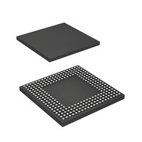
HD6417720BP133BV Renesas Electronics America, HD6417720BP133BV Datasheet - Page 1069

HD6417720BP133BV
Manufacturer Part Number
HD6417720BP133BV
Description
SH3-DSP, WITH USB AND LCDC, PB-F
Manufacturer
Renesas Electronics America
Series
SuperH® SH7700r
Datasheet
1.R8A77210C133BAV.pdf
(1478 pages)
Specifications of HD6417720BP133BV
Core Processor
SH-3 DSP
Core Size
32-Bit
Speed
133MHz
Connectivity
FIFO, I²C, IrDA, MMC, SCI, SD, SIO, SIM, USB
Peripherals
DMA, LCD, POR, WDT
Number Of I /o
117
Program Memory Type
ROMless
Ram Size
16K x 8
Voltage - Supply (vcc/vdd)
1.4 V ~ 1.6 V
Data Converters
A/D 4x10b; D/A 2x8b
Oscillator Type
Internal
Operating Temperature
-20°C ~ 75°C
Package / Case
256-BGA
Lead Free Status / RoHS Status
Lead free / RoHS Compliant
Eeprom Size
-
Program Memory Size
-
- Current page: 1069 of 1478
- Download datasheet (10Mb)
SH7720 Group, SH7721 Group
Table 30.2 Register Settings for Smart Card Interface
• Serial mode register (SCSMR) setting
• Bit rate register (SCBRR) setting
• Serial control register (SCSCR) settings
• Smart card mode register (SCSCMR) settings
R01UH0083EJ0400 Rev. 4.00
Sep 21, 2010
Register
SCSMR
SCBRR
SCSCR
SCTDR
SCSSR
SCRDR
SCSCMR
SCSC2R
SCWAIT
SCGRD
SCSMPL
When the IC card is set for the direct convention, the O/E bit is cleared to 0; for the inverse
convention, it is set to 1.
Sets the bit rate. For the method of computing settings, refer to section 30.4.4, Clocks.
Each interrupt can be enabled and disabled using the TIE, RIE, TEIE, and WAIT_IE bits.
By setting either the TE or RE bit to 1, transmission or reception is selected.
The CKE1 and CKE0 bits are used to select the clock output state. For details, refer to section
30.4.4, Clocks.
When the IC card is set for the direct convention, both the SDIR and SINV bits are cleared to
0; for the inverse convention, both are set to 1. The SMIF bit is always set to 1.
Figure 30.3 below shows the register settings and waveform examples at the start character for
two types of IC cards (a direct-convention type and an inverse-convention type).
For the direct-convention type, the logical level 1 is assigned to the Z state, and the logical
level 0 to the A state, and transmission and reception are performed in LSB-first. The data of
the above start character is then H'3B. Even parity is used according to the smart card
specification, and so the parity bit is 1.
Bit 7
0
0
TIE
SCTD7 SCTD6
TDRE
SCRD7 SCRD6 SCRD5
0
EIO
Bit 6
0
0
RIE
RDRF
LCB
0
SCSMPL10 to SCSMPL0, bits 11 to 15 are 0
PE
Bit 5
0
TE
SCTD5
ORER
PB
0
SCWAIT15 to SCWAIT0
Bit 4
O/E
0
RE
SCTD4 SCTD3
ERS
SCRD4 SCRD3
0
0
SCGRD7 to SCGRD0
Bit 3
0
0
WAIT_IE
PER
SDIR
0
Bit
Bit 2
0
BRR2
TEIE
SCTD2
TEND
SCRD2
SINV
0
Section 30 SIM Card Module (SIM)
Bit 1
0
BRR1
CKE1
SCTD1
WAIT_ER
SCRD1
RST
0
Page 1009 of 1414
Bit 0
0
BRR0
CKE0
SCTD0
0
SCRD0
1
0
Related parts for HD6417720BP133BV
Image
Part Number
Description
Manufacturer
Datasheet
Request
R

Part Number:
Description:
KIT STARTER FOR M16C/29
Manufacturer:
Renesas Electronics America
Datasheet:

Part Number:
Description:
KIT STARTER FOR R8C/2D
Manufacturer:
Renesas Electronics America
Datasheet:

Part Number:
Description:
R0K33062P STARTER KIT
Manufacturer:
Renesas Electronics America
Datasheet:

Part Number:
Description:
KIT STARTER FOR R8C/23 E8A
Manufacturer:
Renesas Electronics America
Datasheet:

Part Number:
Description:
KIT STARTER FOR R8C/25
Manufacturer:
Renesas Electronics America
Datasheet:

Part Number:
Description:
KIT STARTER H8S2456 SHARPE DSPLY
Manufacturer:
Renesas Electronics America
Datasheet:

Part Number:
Description:
KIT STARTER FOR R8C38C
Manufacturer:
Renesas Electronics America
Datasheet:

Part Number:
Description:
KIT STARTER FOR R8C35C
Manufacturer:
Renesas Electronics America
Datasheet:

Part Number:
Description:
KIT STARTER FOR R8CL3AC+LCD APPS
Manufacturer:
Renesas Electronics America
Datasheet:

Part Number:
Description:
KIT STARTER FOR RX610
Manufacturer:
Renesas Electronics America
Datasheet:

Part Number:
Description:
KIT STARTER FOR R32C/118
Manufacturer:
Renesas Electronics America
Datasheet:

Part Number:
Description:
KIT DEV RSK-R8C/26-29
Manufacturer:
Renesas Electronics America
Datasheet:

Part Number:
Description:
KIT STARTER FOR SH7124
Manufacturer:
Renesas Electronics America
Datasheet:

Part Number:
Description:
KIT STARTER FOR H8SX/1622
Manufacturer:
Renesas Electronics America
Datasheet:

Part Number:
Description:
KIT DEV FOR SH7203
Manufacturer:
Renesas Electronics America
Datasheet:


