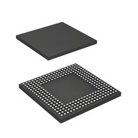
HD6417720BP133BV Renesas Electronics America, HD6417720BP133BV Datasheet - Page 1281

HD6417720BP133BV
Manufacturer Part Number
HD6417720BP133BV
Description
SH3-DSP, WITH USB AND LCDC, PB-F
Manufacturer
Renesas Electronics America
Series
SuperH® SH7700r
Datasheet
1.R8A77210C133BAV.pdf
(1478 pages)
Specifications of HD6417720BP133BV
Core Processor
SH-3 DSP
Core Size
32-Bit
Speed
133MHz
Connectivity
FIFO, I²C, IrDA, MMC, SCI, SD, SIO, SIM, USB
Peripherals
DMA, LCD, POR, WDT
Number Of I /o
117
Program Memory Type
ROMless
Ram Size
16K x 8
Voltage - Supply (vcc/vdd)
1.4 V ~ 1.6 V
Data Converters
A/D 4x10b; D/A 2x8b
Oscillator Type
Internal
Operating Temperature
-20°C ~ 75°C
Package / Case
256-BGA
Lead Free Status / RoHS Status
Lead free / RoHS Compliant
Eeprom Size
-
Program Memory Size
-
- Current page: 1281 of 1478
- Download datasheet (10Mb)
SH7720 Group, SH7721 Group
Table 36.2 H-UDI Commands
36.3.3
Shift register is a 32-bit register. The upper 16 bits are set in SDIR at Update-IR.
If shifted in, the shift-in value is shift-out after the value of the 32-bit shift register is shifted out.
36.3.4
SDBSR is a 434-bit shift register, located on the PAD, for controlling the input/output pins of this
LSI. The initial value is undefined. This register cannot be accessed by the CPU.
Using the EXTEST, SAMPLE/PRELOAD, CLAMP, and HIGHZ commands, a boundary scan
test supporting the JTAG standard can be carried out. Table 36.3 shows the correspondence
between this LSI's pins and boundary scan register bits.
R01UH0083EJ0400 Rev. 4.00
Sep 21, 2010
TI7
0
0
0
0
0
0
1
1
1
TI6
0
0
0
1
1
1
0
1
1
Shift Register
Boundary Scan Register (SDBSR)
TI5
0
1
1
0
1
1
1
1
1
Other than the above
TI4
0
0
1
0
0
1
⎯
0
1
Bits 15 to 8
TI3
⎯
⎯
⎯
⎯
⎯
⎯
⎯
⎯
⎯
TI2
⎯
⎯
⎯
⎯
⎯
⎯
⎯
⎯
⎯
TI1
⎯
⎯
⎯
⎯
⎯
⎯
⎯
⎯
⎯
⎯
⎯
⎯
⎯
⎯
⎯
⎯
⎯
⎯
TI0
Section 36 User Debugging Interface (H-UDI)
Description
JTAG EXTEST
JTAG CLAMP
JTAG HIGHZ
JTAG SAMPLE/PRELOAD
H-UDI reset, negate
H-UDI reset, assert
H-UDI interrupt
JTAG IDCODE (Initial value)
JTAG BYPASS
Reserved
Page 1221 of 1414
Related parts for HD6417720BP133BV
Image
Part Number
Description
Manufacturer
Datasheet
Request
R

Part Number:
Description:
KIT STARTER FOR M16C/29
Manufacturer:
Renesas Electronics America
Datasheet:

Part Number:
Description:
KIT STARTER FOR R8C/2D
Manufacturer:
Renesas Electronics America
Datasheet:

Part Number:
Description:
R0K33062P STARTER KIT
Manufacturer:
Renesas Electronics America
Datasheet:

Part Number:
Description:
KIT STARTER FOR R8C/23 E8A
Manufacturer:
Renesas Electronics America
Datasheet:

Part Number:
Description:
KIT STARTER FOR R8C/25
Manufacturer:
Renesas Electronics America
Datasheet:

Part Number:
Description:
KIT STARTER H8S2456 SHARPE DSPLY
Manufacturer:
Renesas Electronics America
Datasheet:

Part Number:
Description:
KIT STARTER FOR R8C38C
Manufacturer:
Renesas Electronics America
Datasheet:

Part Number:
Description:
KIT STARTER FOR R8C35C
Manufacturer:
Renesas Electronics America
Datasheet:

Part Number:
Description:
KIT STARTER FOR R8CL3AC+LCD APPS
Manufacturer:
Renesas Electronics America
Datasheet:

Part Number:
Description:
KIT STARTER FOR RX610
Manufacturer:
Renesas Electronics America
Datasheet:

Part Number:
Description:
KIT STARTER FOR R32C/118
Manufacturer:
Renesas Electronics America
Datasheet:

Part Number:
Description:
KIT DEV RSK-R8C/26-29
Manufacturer:
Renesas Electronics America
Datasheet:

Part Number:
Description:
KIT STARTER FOR SH7124
Manufacturer:
Renesas Electronics America
Datasheet:

Part Number:
Description:
KIT STARTER FOR H8SX/1622
Manufacturer:
Renesas Electronics America
Datasheet:

Part Number:
Description:
KIT DEV FOR SH7203
Manufacturer:
Renesas Electronics America
Datasheet:


